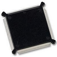
MC68HC16Z1CEH25 Freescale Semiconductor, MC68HC16Z1CEH25 Datasheet - Page 204

MC68HC16Z1CEH25
Manufacturer Part Number
MC68HC16Z1CEH25
Description
IC MCU 16BIT 25MHZ 132-PQFP
Manufacturer
Freescale Semiconductor
Series
HC16r
Datasheet
1.MC68HC16Z1VEH16.pdf
(500 pages)
Specifications of MC68HC16Z1CEH25
Core Processor
CPU16
Core Size
16-Bit
Speed
25MHz
Connectivity
EBI/EMI, SCI, SPI
Peripherals
POR, PWM, WDT
Number Of I /o
16
Program Memory Type
ROMless
Ram Size
1K x 8
Voltage - Supply (vcc/vdd)
2.7 V ~ 5.5 V
Data Converters
A/D 8x10b
Oscillator Type
Internal
Operating Temperature
-40°C ~ 85°C
Package / Case
132-QFP
Package
132PQFP
Family Name
HC16
Maximum Speed
25 MHz
Operating Supply Voltage
3.3|5 V
Data Bus Width
16 Bit
Number Of Programmable I/os
16
On-chip Adc
8-chx10-bit
Number Of Timers
11
Controller Family/series
68HC16
No. Of I/o's
16
Ram Memory Size
1KB
Cpu Speed
25MHz
No. Of Timers
2
Embedded Interface Type
QSPI, SCI
Rohs Compliant
Yes
Processor Series
HC16Z
Core
CPU16
Data Ram Size
1 KB
Interface Type
SCI, SPI, UART
Maximum Clock Frequency
25 MHz
Maximum Operating Temperature
+ 85 C
Mounting Style
SMD/SMT
Minimum Operating Temperature
- 40 C
Lead Free Status / RoHS Status
Lead free / RoHS Compliant
Eeprom Size
-
Program Memory Size
-
Lead Free Status / Rohs Status
Details
Available stocks
Company
Part Number
Manufacturer
Quantity
Price
Company:
Part Number:
MC68HC16Z1CEH25
Manufacturer:
Freescale Semiconductor
Quantity:
135
Company:
Part Number:
MC68HC16Z1CEH25
Manufacturer:
Freescale Semiconductor
Quantity:
10 000
- Current page: 204 of 500
- Download datasheet (6Mb)
8.8.4 Accommodating Positive/Negative Stress Conditions
8-18
Other suggestions for PCB layout in which the ADC is employed include the following:
Positive or negative stress refers to conditions which exceed nominally defined oper-
ating limits. Examples include applying a voltage exceeding the normal limit on an
input (for example, voltages outside of the suggested supply/reference ranges) or
causing currents into or out of the pin which exceed normal limits. ADC specific con-
siderations are voltages greater than V
input which cause excessive currents into or out of the input. Refer to
ELECTRICAL CHARACTERISTICS
Both stress conditions can potentially disrupt conversion results on neighboring inputs.
Parasitic devices, associated with CMOS processes, can cause an immediate disrup-
tive influence on neighboring pins. Common examples of parasitic devices are diodes
to substrate and bipolar devices with the base terminal tied to substrate (V
ground). Under stress conditions, current introduced on an adjacent pin can cause er-
rors on adjacent channels by developing a voltage drop across the adjacent external
channel source impedances.
Figure 8-7
stress conditions. Positive stress conditions do not activate a similar parasitic device.
• The analog ground must be low impedance to all analog ground points in the cir-
• Bypass capacitors should be as close to the power pins as possible.
• The analog ground should be isolated from the digital ground. This can be done
• Non-minimum traces should be utilized for connecting bypass capacitors and
• Minimum distance for trace runs when possible.
cuit.
by cutting a separate ground plane for the analog ground.
filters to their corresponding ground/power points.
This star-point scheme still requires adequate grounding for digital
and analog subsystems in addition to the star-point ground.
shows an active parasitic bipolar when an input pin is subjected to negative
Figure 8-7 Input Pin Subjected to Negative Stress
VDD
Freescale Semiconductor, Inc.
For More Information On This Product,
NEGATIVE
ANALOG-TO-DIGITAL CONVERTER
VOLTAGE
STRESS
+
Go to: www.freescale.com
R
R
ADJACENT
STRESS
on exact magnitudes.
10K
DDA
NOTE
, V
I
OUT
I
IN
RH
PARASITIC
or less than V
DEVICE
PIN UNDER
ADJACENT
STRESS
PINS
SSA
applied to an analog
M68HC16 Z SERIES
USER’S MANUAL
APPENDIX A
ADC PAR STRESS CONN
SSI
/V
SSA
Related parts for MC68HC16Z1CEH25
Image
Part Number
Description
Manufacturer
Datasheet
Request
R
Part Number:
Description:
Manufacturer:
Freescale Semiconductor, Inc
Datasheet:
Part Number:
Description:
Manufacturer:
Freescale Semiconductor, Inc
Datasheet:
Part Number:
Description:
Manufacturer:
Freescale Semiconductor, Inc
Datasheet:
Part Number:
Description:
Manufacturer:
Freescale Semiconductor, Inc
Datasheet:
Part Number:
Description:
Manufacturer:
Freescale Semiconductor, Inc
Datasheet:
Part Number:
Description:
Manufacturer:
Freescale Semiconductor, Inc
Datasheet:
Part Number:
Description:
Manufacturer:
Freescale Semiconductor, Inc
Datasheet:
Part Number:
Description:
Manufacturer:
Freescale Semiconductor, Inc
Datasheet:
Part Number:
Description:
Manufacturer:
Freescale Semiconductor, Inc
Datasheet:
Part Number:
Description:
Manufacturer:
Freescale Semiconductor, Inc
Datasheet:
Part Number:
Description:
Manufacturer:
Freescale Semiconductor, Inc
Datasheet:
Part Number:
Description:
Manufacturer:
Freescale Semiconductor, Inc
Datasheet:
Part Number:
Description:
Manufacturer:
Freescale Semiconductor, Inc
Datasheet:
Part Number:
Description:
Manufacturer:
Freescale Semiconductor, Inc
Datasheet:
Part Number:
Description:
Manufacturer:
Freescale Semiconductor, Inc
Datasheet:


