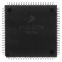
MC9S12D64CPVE Freescale Semiconductor, MC9S12D64CPVE Datasheet - Page 92

MC9S12D64CPVE
Manufacturer Part Number
MC9S12D64CPVE
Description
IC MCU 64K FLASH 25MHZ 112LQFP
Manufacturer
Freescale Semiconductor
Series
HCS12r
Specifications of MC9S12D64CPVE
Core Processor
HCS12
Core Size
16-Bit
Speed
25MHz
Connectivity
CAN, I²C, SCI, SPI
Peripherals
PWM, WDT
Number Of I /o
91
Program Memory Size
64KB (64K x 8)
Program Memory Type
FLASH
Eeprom Size
1K x 8
Ram Size
4K x 8
Voltage - Supply (vcc/vdd)
2.35 V ~ 5.25 V
Data Converters
A/D 16x10b
Oscillator Type
Internal
Operating Temperature
-40°C ~ 85°C
Package / Case
112-LQFP
Processor Series
S12D
Core
HCS12
Data Bus Width
16 bit
Data Ram Size
4 KB
Interface Type
CAN/I2C/SCI/SPI
Maximum Clock Frequency
25 MHz
Number Of Programmable I/os
49
Number Of Timers
8
Maximum Operating Temperature
+ 85 C
Mounting Style
SMD/SMT
3rd Party Development Tools
EWHCS12
Development Tools By Supplier
M68KIT912DP256
Minimum Operating Temperature
- 40 C
On-chip Adc
2 (8-ch x 10-bit)
Lead Free Status / RoHS Status
Lead free / RoHS Compliant
Available stocks
Company
Part Number
Manufacturer
Quantity
Price
Company:
Part Number:
MC9S12D64CPVE
Manufacturer:
Freescale Semiconductor
Quantity:
10 000
Part Number:
MC9S12D64CPVE
Manufacturer:
FREESCALE
Quantity:
20 000
MC9S12DJ64 Device User Guide — V01.20
The total power dissipation can be calculated from:
Two cases with internal voltage regulator enabled and disabled must be considered:
T A
P D
P INT
JA
1. Internal Voltage Regulator disabled
2. Internal voltage regulator enabled
92
P
For R
respectively
I
additionally contains the current flowing into the external loads with output high.
P
DDR
=
=
IO
IO
=
Ambient Temperature, [ C
=
Total Chip Power Dissipation, [W]
is the sum of all output currents on I/O ports associated with VDDX and VDDR.
is the sum of all output currents on I/O ports associated with VDDX and VDDR.
Package Thermal Resistance, [ C/W]
is the current shown in Table A-7 and not the overall current flowing into VDDR, which
DSON
Chip Internal Power Dissipation, [W]
is valid:
P INT
R DSON
=
I DD V DD
P INT
R DSON
=
P IO
P IO
=
V DD5 V OH
----------------------------------- - for outputs driven high
I DDR V DDR
=
P D
+
=
=
I OH
V OL
----------- - for outputs driven low
I DDPLL V DDPLL
I
OL
–
=
i
i
P INT
;
R DSON
R DSON
;
+
+
P IO
I DDA V DDA
I IO
I IO
i
i
2
2
+
I DDA
V DDA


