MC9S12C64CFUE Freescale Semiconductor, MC9S12C64CFUE Datasheet - Page 245
MC9S12C64CFUE
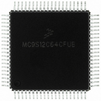
Manufacturer Part Number
MC9S12C64CFUE
Description
IC MCU 64K FLASH 4K RAM 80-QFP
Manufacturer
Freescale Semiconductor
Series
HCS12r
Specifications of MC9S12C64CFUE
Core Processor
HCS12
Core Size
16-Bit
Speed
25MHz
Connectivity
CAN, EBI/EMI, SCI, SPI
Peripherals
POR, PWM, WDT
Number Of I /o
60
Program Memory Size
64KB (64K x 8)
Program Memory Type
FLASH
Ram Size
4K x 8
Voltage - Supply (vcc/vdd)
2.35 V ~ 5.5 V
Data Converters
A/D 8x10b
Oscillator Type
Internal
Operating Temperature
-40°C ~ 85°C
Package / Case
80-QFP
Processor Series
S12C
Core
HCS12
Data Bus Width
16 bit
Data Ram Size
4 KB
Interface Type
CAN/SCI/SPI
Maximum Clock Frequency
25 MHz
Number Of Programmable I/os
60
Number Of Timers
8
Maximum Operating Temperature
+ 85 C
Mounting Style
SMD/SMT
3rd Party Development Tools
EWHCS12
Development Tools By Supplier
M68EVB912C32EE
Minimum Operating Temperature
- 40 C
On-chip Adc
8-ch x 10-bit
Package
80PQFP
Family Name
HCS12
Maximum Speed
25 MHz
Operating Supply Voltage
2.5|5 V
Height
2.4 mm
Length
14 mm
Supply Voltage (max)
2.75 V, 5.5 V
Supply Voltage (min)
2.35 V, 2.97 V
Width
14 mm
Lead Free Status / RoHS Status
Lead free / RoHS Compliant
Eeprom Size
-
Lead Free Status / Rohs Status
Lead free / RoHS Compliant
Available stocks
Company
Part Number
Manufacturer
Quantity
Price

Company:
Part Number:
MC9S12C64CFUE
Manufacturer:
Freescale Semiconductor
Quantity:
10 000


8.4
The ATD10B8C is structured in an analog and a digital sub-block.
8.4.1
The analog sub-block contains all analog electronics required to perform a single conversion. Separate
power supplies V
8.4.1.1
The sample and hold (S/H) machine accepts analog signals from the external surroundings and stores them
as capacitor charge on a storage node.
The sample process uses a two stage approach. During the first stage, the sample amplifier is used to
quickly charge the storage node.The second stage connects the input directly to the storage node to
complete the sample for high accuracy.
When not sampling, the sample and hold machine disables its own clocks. The analog electronics still draw
their quiescent current. The power down (ADPU) bit must be set to disable both the digital clocks and the
analog power consumption.
The input analog signals are unipolar and must fall within the potential range of V
8.4.1.2
The analog input multiplexer connects one of the 8 external analog input channels to the sample and hold
machine.
8.4.1.3
The sample amplifier is used to buffer the input analog signal so that the storage node can be quickly
charged to the sample potential.
8.4.1.4
The A/D machine performs analog-to-digital conversions. The resolution is program selectable at either 8
or 10 bits. The A/D machine uses a successive approximation architecture. It functions by comparing the
stored analog sample potential with a series of digitally generated analog potentials. By following a binary
search algorithm, the A/D machine locates the approximating potential that is nearest to the sampled
potential.
When not converting the A/D machine disables its own clocks. The analog electronics still draws quiescent
current. The power down (ADPU) bit must be set to disable both the digital clocks and the analog power
consumption.
Only analog input signals within the potential range of V
in a non-railed digital output codes.
Freescale Semiconductor
Functional Description
Analog Sub-block
Sample and Hold Machine
Analog Input Multiplexer
Sample Buffer Amplifier
Analog-to-Digital (A/D) Machine
DDA
and V
SSA
allow to isolate noise of other MCU circuitry from the analog sub-block.
MC9S12C-Family / MC9S12GC-Family
Rev 01.24
Chapter 8 Analog-to-Digital Converter (ATD10B8C) Block Description
RL
to V
RH
(A/D reference potentials) will result
SSA
to V
DDA
.
245
Related parts for MC9S12C64CFUE
Image
Part Number
Description
Manufacturer
Datasheet
Request
R

Part Number:
Description:
Manufacturer:
Freescale Semiconductor, Inc
Datasheet:
Part Number:
Description:
Manufacturer:
Freescale Semiconductor, Inc
Datasheet:
Part Number:
Description:
Manufacturer:
Freescale Semiconductor, Inc
Datasheet:
Part Number:
Description:
Manufacturer:
Freescale Semiconductor, Inc
Datasheet:
Part Number:
Description:
Manufacturer:
Freescale Semiconductor, Inc
Datasheet:
Part Number:
Description:
Manufacturer:
Freescale Semiconductor, Inc
Datasheet:
Part Number:
Description:
Manufacturer:
Freescale Semiconductor, Inc
Datasheet:
Part Number:
Description:
Manufacturer:
Freescale Semiconductor, Inc
Datasheet:
Part Number:
Description:
Manufacturer:
Freescale Semiconductor, Inc
Datasheet:
Part Number:
Description:
Manufacturer:
Freescale Semiconductor, Inc
Datasheet:
Part Number:
Description:
Manufacturer:
Freescale Semiconductor, Inc
Datasheet:
Part Number:
Description:
Manufacturer:
Freescale Semiconductor, Inc
Datasheet:
Part Number:
Description:
Manufacturer:
Freescale Semiconductor, Inc
Datasheet:
Part Number:
Description:
Manufacturer:
Freescale Semiconductor, Inc
Datasheet:
Part Number:
Description:
Manufacturer:
Freescale Semiconductor, Inc
Datasheet: