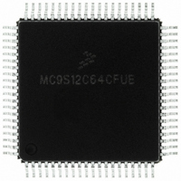
MC9S12C64CFUE Freescale Semiconductor, MC9S12C64CFUE Datasheet - Page 148

MC9S12C64CFUE
Manufacturer Part Number
MC9S12C64CFUE
Description
IC MCU 64K FLASH 4K RAM 80-QFP
Manufacturer
Freescale Semiconductor
Series
HCS12r
Specifications of MC9S12C64CFUE
Core Processor
HCS12
Core Size
16-Bit
Speed
25MHz
Connectivity
CAN, EBI/EMI, SCI, SPI
Peripherals
POR, PWM, WDT
Number Of I /o
60
Program Memory Size
64KB (64K x 8)
Program Memory Type
FLASH
Ram Size
4K x 8
Voltage - Supply (vcc/vdd)
2.35 V ~ 5.5 V
Data Converters
A/D 8x10b
Oscillator Type
Internal
Operating Temperature
-40°C ~ 85°C
Package / Case
80-QFP
Processor Series
S12C
Core
HCS12
Data Bus Width
16 bit
Data Ram Size
4 KB
Interface Type
CAN/SCI/SPI
Maximum Clock Frequency
25 MHz
Number Of Programmable I/os
60
Number Of Timers
8
Maximum Operating Temperature
+ 85 C
Mounting Style
SMD/SMT
3rd Party Development Tools
EWHCS12
Development Tools By Supplier
M68EVB912C32EE
Minimum Operating Temperature
- 40 C
On-chip Adc
8-ch x 10-bit
Package
80PQFP
Family Name
HCS12
Maximum Speed
25 MHz
Operating Supply Voltage
2.5|5 V
Height
2.4 mm
Length
14 mm
Supply Voltage (max)
2.75 V, 5.5 V
Supply Voltage (min)
2.35 V, 2.97 V
Width
14 mm
Lead Free Status / RoHS Status
Lead free / RoHS Compliant
Eeprom Size
-
Lead Free Status / Rohs Status
Lead free / RoHS Compliant
Available stocks
Company
Part Number
Manufacturer
Quantity
Price
Company:
Part Number:
MC9S12C64CFUE
Manufacturer:
Freescale Semiconductor
Quantity:
10 000
- Current page: 148 of 690
- Download datasheet (4Mb)
Chapter 4 Multiplexed External Bus Interface (MEBIV3)
4.3.2.13
This register location is not used (reserved). All bits in this register return logic 0s when read. Writes to
this register have no effect.
This register is not in the on-chip memory map in expanded and special peripheral modes. Therefore, these
accesses will be echoed externally.
4.3.2.14
Read: See individual bit descriptions below
Write: See individual bit descriptions below
148
Module Base + 0x000F
Starting address location affected by INITRG register setting.
Module Base + 0x001E
Starting address location affected by INITRG register setting.
IRQEN
Field
IRQE
7
6
Reset
Reset
W
W
R
R
IRQ Select Edge Sensitive Only
Special modes: read or write anytime
Normal and Emulation modes: read anytime, write once
0 IRQ configured for low level recognition.
1 IRQ configured to respond only to falling edges. Falling edges on the IRQ pin will be detected anytime
External IRQ Enable
Normal, emulation, and special modes: read or write anytime
0 External IRQ pin is disconnected from interrupt logic.
1 External IRQ pin is connected to interrupt logic.
Note: When IRQEN = 0, the edge detect latch is disabled.
Reserved Register
IRQ Control Register (IRQCR)
IRQE = 1 and will be cleared only upon a reset or the servicing of the IRQ interrupt.
IRQE
7
0
0
7
0
= Unimplemented or Reserved
= Unimplemented or Reserved
IRQEN
6
0
0
6
1
Figure 4-18. IRQ Control Register (IRQCR)
Table 4-12. IRQCR Field Descriptions
MC9S12C-Family / MC9S12GC-Family
Figure 4-17. Reserved Register
5
0
0
5
0
0
Rev 01.24
0
0
0
0
Description
4
4
0
0
0
0
3
3
0
0
0
0
2
2
Freescale Semiconductor
0
0
0
0
1
1
0
0
0
0
0
0
Related parts for MC9S12C64CFUE
Image
Part Number
Description
Manufacturer
Datasheet
Request
R
Part Number:
Description:
Manufacturer:
Freescale Semiconductor, Inc
Datasheet:
Part Number:
Description:
Manufacturer:
Freescale Semiconductor, Inc
Datasheet:
Part Number:
Description:
Manufacturer:
Freescale Semiconductor, Inc
Datasheet:
Part Number:
Description:
Manufacturer:
Freescale Semiconductor, Inc
Datasheet:
Part Number:
Description:
Manufacturer:
Freescale Semiconductor, Inc
Datasheet:
Part Number:
Description:
Manufacturer:
Freescale Semiconductor, Inc
Datasheet:
Part Number:
Description:
Manufacturer:
Freescale Semiconductor, Inc
Datasheet:
Part Number:
Description:
Manufacturer:
Freescale Semiconductor, Inc
Datasheet:
Part Number:
Description:
Manufacturer:
Freescale Semiconductor, Inc
Datasheet:
Part Number:
Description:
Manufacturer:
Freescale Semiconductor, Inc
Datasheet:
Part Number:
Description:
Manufacturer:
Freescale Semiconductor, Inc
Datasheet:
Part Number:
Description:
Manufacturer:
Freescale Semiconductor, Inc
Datasheet:
Part Number:
Description:
Manufacturer:
Freescale Semiconductor, Inc
Datasheet:
Part Number:
Description:
Manufacturer:
Freescale Semiconductor, Inc
Datasheet:
Part Number:
Description:
Manufacturer:
Freescale Semiconductor, Inc
Datasheet:


