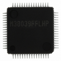
M38039FFLHP#U0 Renesas Electronics America, M38039FFLHP#U0 Datasheet - Page 72

M38039FFLHP#U0
Manufacturer Part Number
M38039FFLHP#U0
Description
IC 3803 MCU FLASH 64LQFP
Manufacturer
Renesas Electronics America
Series
740/38000r
Datasheet
1.M38039FFLHPU0.pdf
(121 pages)
Specifications of M38039FFLHP#U0
Core Processor
740
Core Size
8-Bit
Speed
16.8MHz
Connectivity
SIO, UART/USART
Peripherals
PWM, WDT
Number Of I /o
56
Program Memory Size
60KB (60K x 8)
Program Memory Type
FLASH
Ram Size
2K x 8
Voltage - Supply (vcc/vdd)
2.7 V ~ 5.5 V
Data Converters
A/D 16x10b; D/A 2x8b
Oscillator Type
Internal
Operating Temperature
-20°C ~ 85°C
Package / Case
64-LQFP
Lead Free Status / RoHS Status
Lead free / RoHS Compliant
Eeprom Size
-
Available stocks
Company
Part Number
Manufacturer
Quantity
Price
3803 Group (Spec.L)
Rev.1.01
REJ03B0212-0101
Boot Mode
The control program for CPU rewrite mode must be written into
the User ROM or Boot ROM area in parallel I/O mode
beforehand. (If the control program is written into the Boot ROM
area, the standard serial I/O mode becomes unusable.)
See Figure 67 for details about the Boot ROM area.
N o r m a l m i c r o c o m p u t e r m o d e i s e n t e r e d w h e n t h e
microcomputer is reset with pulling CNV
the CPU starts operating using the control program in the User
ROM area.
When the microcomputer is reset and the CNV
pulling the P4
operating (start address of program is stored into addresses
FFFC
ROM area. This mode is called the “Boot mode”. Also, User
ROM area can be rewritten using the control program in the Boot
ROM area.
Block Address
Block addresses refer to the maximum address of each block.
These addresses are used in the block erase command.
Fig 67. Block diagram of built-in flash memory
16
RAM
and FFFD
Jan 25, 2008
FFFF
0FE0
0FFF
083F
5
0000
0040
1000
/TxD
16
16
16
16
16
16
16
16
1
) using the control program in the Boot
Internal flash memory area
pin and CNV
Internal RAM area
(60 Kbytes)
(2 Kbytes)
SFR area
SFR area
Page 70 of 117
SS
pin high, the CPU starts
SS
pin low. In this case,
SS
pin high after
FFFF
C000
E000
1000
1800
2000
8000
16
16
16
16
16
16
16
CPU Rewrite Mode
In CPU rewrite mode, the internal flash memory can be operated
on (read, program, or erase) under control of the Central
Processing Unit (CPU).
In CPU rewrite mode, only the User ROM area shown in Figure
67 can be rewritten; the Boot ROM area cannot be rewritten.
Make sure the program and block erase commands are issued for
only the User ROM area and each block area.
The control program for CPU rewrite mode can be stored in
either User ROM or Boot ROM area. In the CPU rewrite mode,
because the flash memory cannot be read from the CPU, the
rewrite control program must be transferred to internal RAM
area before it can be executed.
Block 3: 24 Kbytes
Block 2: 16 Kbytes
Block 0: 8 Kbytes
Block 1: 8 Kbytes
User ROM area
Data block B:
Data block A:
2 Kbytes
2 Kbytes
Notes 1: The boot ROM area can be rewritten
2: To specify a block, use the maximum
3: The mask ROM version has the
FFFF
(Access to except boot ROM area is
disabled.)
reserved
difference of the area.
F000
16
16
in
address in the block.
ROM
a
Boot ROM area
parallel
4 Kbytes
area.
I/O
Note
mode.
the


