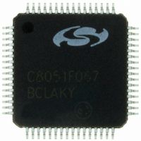
C8051F067-GQ Silicon Laboratories Inc, C8051F067-GQ Datasheet - Page 79

C8051F067-GQ
Manufacturer Part Number
C8051F067-GQ
Description
IC 8051 MCU 32K FLASH 64TQFP
Manufacturer
Silicon Laboratories Inc
Series
C8051F06xr
Specifications of C8051F067-GQ
Core Processor
8051
Core Size
8-Bit
Speed
25MHz
Connectivity
SMBus (2-Wire/I²C), SPI, UART/USART
Peripherals
Brown-out Detect/Reset, POR, PWM, WDT
Number Of I /o
24
Program Memory Size
32KB (32K x 8)
Program Memory Type
FLASH
Ram Size
4.25K x 8
Voltage - Supply (vcc/vdd)
2.7 V ~ 3.6 V
Data Converters
A/D 2x16b
Oscillator Type
Internal
Operating Temperature
-40°C ~ 85°C
Package / Case
64-TQFP, 64-VQFP
Processor Series
C8051F0x
Core
8051
Data Bus Width
8 bit
Data Ram Size
4.25 KB
Interface Type
I2C, SMBus, SPI, UART
Maximum Clock Frequency
25 MHz
Number Of Programmable I/os
24
Number Of Timers
5
Operating Supply Voltage
2.7 V to 3.6 V
Maximum Operating Temperature
+ 85 C
Mounting Style
SMD/SMT
3rd Party Development Tools
PK51, CA51, A51, ULINK2
Development Tools By Supplier
C8051F060DK
Minimum Operating Temperature
- 40 C
On-chip Adc
16 bit, 1 Channel
On-chip Dac
12 bit, 2 Channel
Lead Free Status / RoHS Status
Lead free / RoHS Compliant
Eeprom Size
-
Lead Free Status / Rohs Status
Details
Other names
336-1222
Available stocks
Company
Part Number
Manufacturer
Quantity
Price
Company:
Part Number:
C8051F067-GQ
Manufacturer:
AD
Quantity:
210
Company:
Part Number:
C8051F067-GQ
Manufacturer:
Silicon Laboratories Inc
Quantity:
10 000
Company:
Part Number:
C8051F067-GQR
Manufacturer:
Silicon Laboratories Inc
Quantity:
10 000
- Current page: 79 of 328
- Download datasheet (2Mb)
6.6.
The DMA contains multiple interrupt sources. Some of these can be individually enabled to generate inter-
rupts as necessary. The DMA Control Register (DMA0CN, Figure 6.4) and DMA Configuration Register
(DMA0CF, Figure 6.5) contain the enable bits and flags for the DMA interrupt sources. When an interrupt is
enabled and the interrupt condition occurs, a DMA interrupt will be generated (EIE2.7 is set to ‘1’).
The DMA flags that can generate a DMA0 interrupt are:
6.7.
The data paths from the ADCs to XRAM are double-buffered when using the DMA interface. When a con-
version is completed by the ADC, it first enters the ADCs data register. If the DMA’s data buffer is empty,
the conversion results will immediately be written into the DMA’s internal data buffer for that ADC. Data in
the DMA’s internal data buffer is written to XRAM at the first available opportunity (see
Addressing and Setup” on page
the DMA’s data buffer until data in the buffer has been written to XRAM. When a conversion is completed
and the DMA’s data buffer is not empty, an overflow warning flag is generated. If a second conversion data
word becomes available before the DMA’s data buffer is written to XRAM, the data in the ADC’s data regis-
ters is over-written with the new data word, and a data overflow error flag is generated.
Interrupt Sources
1. DMA Operations Complete (DMA0CN.6, DMA0INT) occurs when all DMA operations have
2. ADC1 Data Overflow Error (DMA0CN.4, DMA0DE1) occurs when the DMA interface cannot
3. ADC0 Data Overflow Error (DMA0CN.3, DMA0DE0) occurs when the DMA interface cannot
4. ADC1 Data Overflow Warning (DMA0CN.1, DMA0DO1) occurs when data from ADC0
5. ADC0 Data Overflow Warning (DMA0CN.0, DMA0DO0) occurs when data from ADC1
6. Repeat Counter Overflow (DMA0CF.2, DMA0CI) occurs when the Repeat Counter reaches
7. End Of Operation (DMA0CF.0, DMA0EO) occurs when an End Of Operation instruction is
Data Buffer Overflow Warnings and Errors
been completed, and the DMA interface is idle.
access XRAM for two conversion cycles of ADC1. This flag indicates that at least one conver-
sion result from ADC1 has been discarded.
access XRAM for two conversion cycles of ADC0. This flag indicates that at least one conver-
sion result from ADC0 has been discarded.
becomes available and the DMA has not yet written the previous results to XRAM. This inter-
rupt source can be enabled and disabled with the Data Overflow Warning Enable bit
(DMA0CN.2, DMA0DOE).
becomes available and the DMA has not yet written the previous results to XRAM. This inter-
rupt source can be enabled and disabled with the Data Overflow Warning Enable bit
(DMA0CN.2, DMA0DOE).
the Repeat Counter Limit. This interrupt source can be enabled and disabled with the Repeat
Counter Overflow Interrupt Enable bit (DMA0CF.3, DMA0CIE).
reached in the Instruction Buffer. This interrupt source can be enabled and disabled with the
End Of Operation Interrupt Enable bit (DMA0CF.1, DMA0EOE).
76). Conversion results from the ADC’s data registers are not copied into
Rev. 1.2
C8051F060/1/2/3/4/5/6/7
Section “6.3. XRAM
79
Related parts for C8051F067-GQ
Image
Part Number
Description
Manufacturer
Datasheet
Request
R
Part Number:
Description:
SMD/C°/SINGLE-ENDED OUTPUT SILICON OSCILLATOR
Manufacturer:
Silicon Laboratories Inc
Part Number:
Description:
Manufacturer:
Silicon Laboratories Inc
Datasheet:
Part Number:
Description:
N/A N/A/SI4010 AES KEYFOB DEMO WITH LCD RX
Manufacturer:
Silicon Laboratories Inc
Datasheet:
Part Number:
Description:
N/A N/A/SI4010 SIMPLIFIED KEY FOB DEMO WITH LED RX
Manufacturer:
Silicon Laboratories Inc
Datasheet:
Part Number:
Description:
N/A/-40 TO 85 OC/EZLINK MODULE; F930/4432 HIGH BAND (REV E/B1)
Manufacturer:
Silicon Laboratories Inc
Part Number:
Description:
EZLink Module; F930/4432 Low Band (rev e/B1)
Manufacturer:
Silicon Laboratories Inc
Part Number:
Description:
I°/4460 10 DBM RADIO TEST CARD 434 MHZ
Manufacturer:
Silicon Laboratories Inc
Part Number:
Description:
I°/4461 14 DBM RADIO TEST CARD 868 MHZ
Manufacturer:
Silicon Laboratories Inc
Part Number:
Description:
I°/4463 20 DBM RFSWITCH RADIO TEST CARD 460 MHZ
Manufacturer:
Silicon Laboratories Inc
Part Number:
Description:
I°/4463 20 DBM RADIO TEST CARD 868 MHZ
Manufacturer:
Silicon Laboratories Inc
Part Number:
Description:
I°/4463 27 DBM RADIO TEST CARD 868 MHZ
Manufacturer:
Silicon Laboratories Inc
Part Number:
Description:
I°/4463 SKYWORKS 30 DBM RADIO TEST CARD 915 MHZ
Manufacturer:
Silicon Laboratories Inc
Part Number:
Description:
N/A N/A/-40 TO 85 OC/4463 RFMD 30 DBM RADIO TEST CARD 915 MHZ
Manufacturer:
Silicon Laboratories Inc
Part Number:
Description:
I°/4463 20 DBM RADIO TEST CARD 169 MHZ
Manufacturer:
Silicon Laboratories Inc


