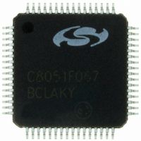
C8051F067-GQ Silicon Laboratories Inc, C8051F067-GQ Datasheet - Page 205

C8051F067-GQ
Manufacturer Part Number
C8051F067-GQ
Description
IC 8051 MCU 32K FLASH 64TQFP
Manufacturer
Silicon Laboratories Inc
Series
C8051F06xr
Specifications of C8051F067-GQ
Core Processor
8051
Core Size
8-Bit
Speed
25MHz
Connectivity
SMBus (2-Wire/I²C), SPI, UART/USART
Peripherals
Brown-out Detect/Reset, POR, PWM, WDT
Number Of I /o
24
Program Memory Size
32KB (32K x 8)
Program Memory Type
FLASH
Ram Size
4.25K x 8
Voltage - Supply (vcc/vdd)
2.7 V ~ 3.6 V
Data Converters
A/D 2x16b
Oscillator Type
Internal
Operating Temperature
-40°C ~ 85°C
Package / Case
64-TQFP, 64-VQFP
Processor Series
C8051F0x
Core
8051
Data Bus Width
8 bit
Data Ram Size
4.25 KB
Interface Type
I2C, SMBus, SPI, UART
Maximum Clock Frequency
25 MHz
Number Of Programmable I/os
24
Number Of Timers
5
Operating Supply Voltage
2.7 V to 3.6 V
Maximum Operating Temperature
+ 85 C
Mounting Style
SMD/SMT
3rd Party Development Tools
PK51, CA51, A51, ULINK2
Development Tools By Supplier
C8051F060DK
Minimum Operating Temperature
- 40 C
On-chip Adc
16 bit, 1 Channel
On-chip Dac
12 bit, 2 Channel
Lead Free Status / RoHS Status
Lead free / RoHS Compliant
Eeprom Size
-
Lead Free Status / Rohs Status
Details
Other names
336-1222
Available stocks
Company
Part Number
Manufacturer
Quantity
Price
Company:
Part Number:
C8051F067-GQ
Manufacturer:
AD
Quantity:
210
Company:
Part Number:
C8051F067-GQ
Manufacturer:
Silicon Laboratories Inc
Quantity:
10 000
Company:
Part Number:
C8051F067-GQR
Manufacturer:
Silicon Laboratories Inc
Quantity:
10 000
- Current page: 205 of 328
- Download datasheet (2Mb)
18.1. Ports 0 through 3 and the Priority Crossbar Decoder
The Priority Crossbar Decoder, or “Crossbar”, allocates and assigns Port pins on Port 0 through Port 3 to
the digital peripherals (UARTs, SMBus, PCA, Timers, etc.) on the device using a priority order. The Port
pins are allocated in order starting with P0.0 and continue through P3.7 (on the C8051F060/2/4/6) or P2.7
(on the C8051F061/3/5/7) if necessary. The digital peripherals are assigned Port pins in a priority order
which is listed in Figure 18.3, with UART0 having the highest priority and CNVSTR2 having the lowest pri-
ority.
18.1.1. Crossbar Pin Assignment and Allocation
The Crossbar assigns Port pins to a peripheral if the corresponding enable bits of the peripheral are set to
a logic 1 in the Crossbar configuration registers XBR0, XBR1, XBR2, and XBR3, shown in Figure 18.5,
Figure 18.6, Figure 18.7, and Figure 18.8. For example, if the UART0EN bit (XBR0.2) is set to a logic 1,
the TX0 and RX0 pins will be mapped to P0.0 and P0.1 respectively. Because UART0 has the highest pri-
ority, its pins will always be mapped to P0.0 and P0.1 when UART0EN is set to a logic 1. If a digital periph-
TX0
RX0
SCK
MISO
MOSI
NSS
SDA
SCL
TX1
RX1
CEX0
CEX1
CEX2
CEX3
CEX4
CEX5
ECI
CP0
CP1
CP2
T0
/INT0
T1
/INT1
T2
T2EX
T3
T3EX
T4
T4EX
/SYSCLK
CNVSTR2
PIN I/O 0
1
2
3
P0
4
5
6
NSS is not assigned to a port pin when the SPI is placed in 3-wire mode
7
0
Figure 18.3. Priority Crossbar Decode Table
1
2
(P1MDIN = 0xFF; P2MDIN = 0xFF)
3
P1
4
5
6
7
0
Rev. 1.2
1
2
C8051F060/1/2/3/4/5/6/7
3
P2
4
5
6
7
0
1
2
3
P3
4
5
6
7
Crossbar Register Bits
UART0EN:
UART1EN:
CNVSTE2: XBR3.2
SMB0EN:
PCA0ME:
SYSCKE: XBR1.7
SPI0EN:
T2EXE: XBR1.6
T3EXE: XBR3.1
T4EXE: XBR2.4
ECI0E: XBR0.6
INT0E: XBR1.2
INT1E: XBR1.4
CP0E: XBR0.7
CP1E: XBR1.0
CP2E: XBR3.3
T0E: XBR1.1
T1E: XBR1.3
T2E: XBR1.5
T3E: XBR3.0
T4E: XBR2.3
XBR0.2
XBR0.1
XBR0.0
XBR2.2
XBR0.[5:3]
205
Related parts for C8051F067-GQ
Image
Part Number
Description
Manufacturer
Datasheet
Request
R
Part Number:
Description:
SMD/C°/SINGLE-ENDED OUTPUT SILICON OSCILLATOR
Manufacturer:
Silicon Laboratories Inc
Part Number:
Description:
Manufacturer:
Silicon Laboratories Inc
Datasheet:
Part Number:
Description:
N/A N/A/SI4010 AES KEYFOB DEMO WITH LCD RX
Manufacturer:
Silicon Laboratories Inc
Datasheet:
Part Number:
Description:
N/A N/A/SI4010 SIMPLIFIED KEY FOB DEMO WITH LED RX
Manufacturer:
Silicon Laboratories Inc
Datasheet:
Part Number:
Description:
N/A/-40 TO 85 OC/EZLINK MODULE; F930/4432 HIGH BAND (REV E/B1)
Manufacturer:
Silicon Laboratories Inc
Part Number:
Description:
EZLink Module; F930/4432 Low Band (rev e/B1)
Manufacturer:
Silicon Laboratories Inc
Part Number:
Description:
I°/4460 10 DBM RADIO TEST CARD 434 MHZ
Manufacturer:
Silicon Laboratories Inc
Part Number:
Description:
I°/4461 14 DBM RADIO TEST CARD 868 MHZ
Manufacturer:
Silicon Laboratories Inc
Part Number:
Description:
I°/4463 20 DBM RFSWITCH RADIO TEST CARD 460 MHZ
Manufacturer:
Silicon Laboratories Inc
Part Number:
Description:
I°/4463 20 DBM RADIO TEST CARD 868 MHZ
Manufacturer:
Silicon Laboratories Inc
Part Number:
Description:
I°/4463 27 DBM RADIO TEST CARD 868 MHZ
Manufacturer:
Silicon Laboratories Inc
Part Number:
Description:
I°/4463 SKYWORKS 30 DBM RADIO TEST CARD 915 MHZ
Manufacturer:
Silicon Laboratories Inc
Part Number:
Description:
N/A N/A/-40 TO 85 OC/4463 RFMD 30 DBM RADIO TEST CARD 915 MHZ
Manufacturer:
Silicon Laboratories Inc
Part Number:
Description:
I°/4463 20 DBM RADIO TEST CARD 169 MHZ
Manufacturer:
Silicon Laboratories Inc


