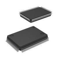
R5F363AENFA#U0 Renesas Electronics America, R5F363AENFA#U0 Datasheet - Page 74

R5F363AENFA#U0
Manufacturer Part Number
R5F363AENFA#U0
Description
MCU 4KB FLASH 256/16K 100-QFP
Manufacturer
Renesas Electronics America
Series
M16C/60/63r
Specifications of R5F363AENFA#U0
Core Processor
M16C/60
Core Size
16/32-Bit
Speed
20MHz
Connectivity
EBI/EMI, I²C, SIO, UART/USART
Peripherals
DMA, LVD, POR, PWM, WDT
Number Of I /o
85
Program Memory Size
256KB (256K x 8)
Program Memory Type
FLASH
Ram Size
20K x 8
Voltage - Supply (vcc/vdd)
1.8 V ~ 5.5 V
Data Converters
A/D 26x10b; D/A 2x8b
Oscillator Type
Internal
Operating Temperature
-20°C ~ 85°C
Package / Case
100-QFP
Lead Free Status / RoHS Status
Lead free / RoHS Compliant
Eeprom Size
-
Available stocks
Company
Part Number
Manufacturer
Quantity
Price
M16C/63 Group
REJ03B0271-0100 Rev.1.00 Sep 15, 2009
Page 72 of 113
5.2.4
Table 5.35
Notes:
t
t
t
t
t
t
t
t
t
t
t
t
t
t
t
t
t
d(BCLK-AD)
h(BCLK-AD)
h(RD-AD)
h(WR-AD)
d(BCLK-CS)
h(BCLK-CS)
d(BCLK-ALE)
h(BCLK-ALE)
d(BCLK-RD)
h(BCLK-RD)
d(BCLK-WR)
h(BCLK-WR)
d(BCLK-DB)
h(BCLK-DB)
d(DB-WR)
h(WR-DB)
d(BCLK-HLDA)
5.2.4.1
1.
2.
3.
Symbol
(V
CC1
Calculated according to the BCLK frequency as follows:
Calculated according to the BCLK frequency as follows:
This standard value shows the timing when the output is off, and does not
show hold time of data bus.
Hold time of data bus varies with capacitor volume and pull-up (pull-down)
resistance value.
Hold time of data bus is expressed in
t = − CR × ln(1 − V
by a circuit of the right figure.
For example, when V
low level is
t = − 30 pF × 1 k Ω × In(1 − 0.2V
0.5 10
--------------------- - 40 ns
0.5 10
--------------------- - 10 ns
f
f
= 6.7 ns.
(
(
BCLK
BCLK
×
×
= V
Switching Characteristics (Memory Expansion Mode and Microprocessor
Mode)
)
)
9
9
Address output delay time
Address output hold time (in relation to BCLK)
Address output hold time (in relation to RD)
Address output hold time (in relation to WR)
Chip select output delay time
Chip select output hold time (in relation to BCLK)
ALE signal output delay time
ALE signal output hold time
RD signal output delay time
RD signal output hold time
WR signal output delay time
WR signal output hold time
Data output delay time (in relation to BCLK)
Data output hold time (in relation to BCLK)
Data output delay time (in relation to WR)
Data output hold time (in relation to WR)
HLDA output delay time
CC2
In No Wait State Setting
Memory Expansion Mode and Microprocessor Mode (in No Wait State Setting)
–
–
= 5 V, V
[
[
]
]
OL
f
(BCLK)
/V
SS
OL
CC2
= 0.2V
= 0 V, at T
)
is 12.5 MHz or less.
CC2
CC2
Parameter
, C = 30 pF, R = 1 k Ω , hold time of output
/V
opr
CC2
= -20 to 85 ° C/-40 to 85 ° C unless otherwise specified)
)
(3)
(3)
Figure 5.14
Measuring
Condition
See
(Note 2)
(Note 1)
(Note 2)
Min.
5. Electrical Characteristics
− 4
0
0
0
0
0
0
Standard
V
CC1
DBi
Max.
= V
25
25
15
25
25
40
40
CC2
= 5 V
Unit
ns
ns
ns
ns
ns
ns
ns
ns
ns
ns
ns
ns
ns
ns
ns
ns
ns
C
R


