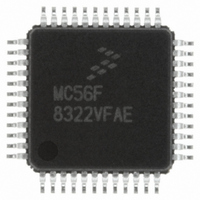
MC56F8322VFAE Freescale Semiconductor, MC56F8322VFAE Datasheet - Page 20

MC56F8322VFAE
Manufacturer Part Number
MC56F8322VFAE
Description
IC DSP 16BIT 60MHZ 48-LQFP
Manufacturer
Freescale Semiconductor
Series
56F8xxxr
Datasheet
1.MC56F8122VFAE.pdf
(136 pages)
Specifications of MC56F8322VFAE
Core Processor
56800
Core Size
16-Bit
Speed
60MHz
Connectivity
CAN, SCI, SPI
Peripherals
POR, PWM, Temp Sensor, WDT
Number Of I /o
21
Program Memory Size
40KB (20K x 16)
Program Memory Type
FLASH
Ram Size
6K x 16
Voltage - Supply (vcc/vdd)
2.25 V ~ 3.6 V
Data Converters
A/D 6x12b
Oscillator Type
Internal
Operating Temperature
-40°C ~ 105°C
Package / Case
48-LQFP
Data Bus Width
16 bit
Processor Series
MC56F83xx
Core
56800E
Numeric And Arithmetic Format
Fixed-Point
Device Million Instructions Per Second
40 MIPs
Maximum Clock Frequency
60 MHz
Number Of Programmable I/os
21
Data Ram Size
4 KB
Operating Supply Voltage
3.3 V
Maximum Operating Temperature
+ 105 C
Mounting Style
SMD/SMT
Interface Type
SCI, SPI, CAN
Minimum Operating Temperature
- 40 C
For Use With
MC56F8323EVME - BOARD EVALUATION MC56F8323
Lead Free Status / RoHS Status
Lead free / RoHS Compliant
Eeprom Size
-
Lead Free Status / Rohs Status
Lead free / RoHS Compliant
Available stocks
Company
Part Number
Manufacturer
Quantity
Price
Company:
Part Number:
MC56F8322VFAE
Manufacturer:
Freescale Semiconductor
Quantity:
10 000
Part Number:
MC56F8322VFAE
Manufacturer:
FREESCALE
Quantity:
20 000
Company:
Part Number:
MC56F8322VFAER2
Manufacturer:
Freescale Semiconductor
Quantity:
10 000
20
Signal Name
(GPIOC0)
(GPIOC1)
EXTAL
XTAL
TMS
TDO
TCK
TDI
Table 2-2 Signal and Package Information for the 48-Pin LQFP (Continued)
Pin No.
32
33
39
40
41
42
Schmitt
Schmitt
Schmitt
Schmitt
Schmitt
Output
Output
Output
Output
Input/
Input/
Input/
Type
Input
Input
Input
State During
low internally
Input, pulled
Input, pulled
Input, pulled
internally
internally
disabled,
pull-up is
output is
In reset,
enabled
Output
Reset
56F8322 Techncial Data, Rev. 16
Input
high
high
External Crystal Oscillator Input — This input can be connected to
an 8MHz external crystal. If an external clock is used, XTAL must be
used as the input and EXTAL connected to V
The input clock can be selected to provide the clock directly to the
core. This input clock can also be selected as the input clock for the
on-chip PLL.
Port C GPIO — This GPIO pin can be individually programmed as an
input or output pin.
After reset, the default state is an EXTAL input with pull-ups disabled.
Crystal Oscillator Output — This output connects the internal crystal
oscillator output to an external crystal.
If an external clock is used, XTAL must be used as the input and
EXTAL connected to V
The input clock can be selected to provide the clock directly to the
core. This input clock can also be selected as the input clock for the
on-chip PLL.
Port C GPIO — This GPIO pin can be individually programmed as an
input or output pin.
After reset, the default state is an XTAL input with pull-ups disabled.
Test Clock Input — This input pin provides a gated clock to
synchronize the test logic and shift serial data to the JTAG/EOnCE
port. The pin is connected internally to a pull-down resistor. A Schmitt
trigger input is used for noise immunity.
Test Mode Select Input — This input pin is used to sequence the
JTAG TAP controller’s state machine. It is sampled on the rising edge
of TCK and has an on-chip pull-up resistor.
Note:
Test Data Input — This input pin provides a serial input data stream
to the JTAG/EOnCE port. It is sampled on the rising edge of TCK and
has an on-chip pull-up resistor.
Test Data Output — This tri-stateable output pin provides a serial
output data stream from the JTAG/EOnCE port. It is driven in the
shift-IR and shift-DR controller states, and changes on the falling edge
of TCK.
Always tie the TMS pin to V
SS
Signal Description
.
DD
through a 2.2K resistor.
Freescale Semiconductor
SS
.
Preliminary


