MC9S12C32CFAE16 Freescale Semiconductor, MC9S12C32CFAE16 Datasheet - Page 447
MC9S12C32CFAE16
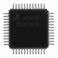
Manufacturer Part Number
MC9S12C32CFAE16
Description
IC MCU 32K FLASH 16MHZ 48-LQFP
Manufacturer
Freescale Semiconductor
Series
HCS12r
Datasheets
1.MC9S12GC16MFUE.pdf
(690 pages)
2.MC9S12C96CFUER.pdf
(26 pages)
3.MC9S12C32CFAE25.pdf
(2 pages)
Specifications of MC9S12C32CFAE16
Core Processor
HCS12
Core Size
16-Bit
Speed
16MHz
Connectivity
CAN, EBI/EMI, SCI, SPI
Peripherals
POR, PWM, WDT
Number Of I /o
31
Program Memory Size
32KB (32K x 8)
Program Memory Type
FLASH
Ram Size
2K x 8
Voltage - Supply (vcc/vdd)
2.35 V ~ 5.5 V
Data Converters
A/D 8x10b
Oscillator Type
Internal
Operating Temperature
-40°C ~ 85°C
Package / Case
48-LQFP
Cpu Family
HCS12
Device Core Size
16b
Frequency (max)
16MHz
Interface Type
CAN/SCI/SPI
Total Internal Ram Size
2KB
# I/os (max)
31
Number Of Timers - General Purpose
8
Operating Supply Voltage (typ)
2.5/5V
Operating Supply Voltage (max)
2.75/5.5V
Operating Supply Voltage (min)
2.35/2.97V
On-chip Adc
8-chx10-bit
Instruction Set Architecture
CISC
Operating Temp Range
-40C to 85C
Operating Temperature Classification
Industrial
Mounting
Surface Mount
Pin Count
48
Package Type
LQFP
Package
48LQFP
Family Name
HCS12
Maximum Speed
16 MHz
Operating Supply Voltage
2.5|5 V
Data Bus Width
16 Bit
Number Of Programmable I/os
31
Number Of Timers
8
For Use With
CML12C32SLK - KIT STUDENT LEARNING 16BIT HCS12
Lead Free Status / RoHS Status
Lead free / RoHS Compliant
Eeprom Size
-
Lead Free Status / Rohs Status
Compliant
Available stocks
Company
Part Number
Manufacturer
Quantity
Price

Company:
Part Number:
MC9S12C32CFAE16
Manufacturer:
Freescale Semiconductor
Quantity:
10 000


Read: Anytime
Write: Anytime
To operate the 16-bit pulse accumulator independently of input capture or output compare 7 and 0
respectively the user must set the corresponding bits IOSx = 1, OMx = 0 and OLx = 0. OC7M7 in the
OC7M register must also be cleared.
To enable output action using the OM7 and OL7 bits on the timer port,the corresponding bit OC7M7 in
the OC7M register must also be cleared. The settings for these bits can be seen in
Freescale Semiconductor
Module Base + 0x0009
IOCx=OC7Dx
IOC7=OM7/O
TC7=TCx
Reset
Field
OMx
OLx
7:0
7:0
L7
W
R
OC7Mx=1
OM3
Output Mode — These eight pairs of control bits are encoded to specify the output action to be taken as a result
of a successful OCx compare. When either OMx or OLx is 1, the pin associated with OCx becomes an output
tied to OCx.
Note: To enable output action by OMx bits on timer port, the corresponding bit in OC7M should be cleared.
Output Level — These eight pairs of control bits are encoded to specify the output action to be taken as a result
of a successful OCx compare. When either OMx or OLx is 1, the pin associated with OCx becomes an output
tied to OCx.
Note: To enable output action by OLx bits on timer port, the corresponding bit in OC7M should be cleared.
0
7
IOCx=OC7Dx
IOC7=OM7/O
+OMx/OLx
TC7>TCx
L7
OC7M7=0
OMx
OL3
0
6
0
0
1
1
TC7=TCx
Figure 15-15. Timer Control Register 2 (TCTL2)
Table 15-11. The OC7 and OCx event priority
Table 15-9. TCTL1/TCTL2 Field Descriptions
Table 15-10. Compare Result Output Action
IOC7=OM7/OL7
IOCx=OMx/OLx
OC7Mx=0
MC9S12C-Family / MC9S12GC-Family
OM2
OLx
0
1
0
1
0
5
TC7>TCx
Timer disconnected from output pin logic
Rev 01.24
OL2
0
4
Clear OCx output line to zero
IOC7=OC7D7
IOCx=OC7Dx
Description
Set OCx output line to one
Toggle OCx output line
TC7=TCx
Chapter 15 Timer Module (TIM16B8CV1) Block Description
OM1
OC7Mx=1
Action
0
3
IOC7=OC7D7
IOCx=OC7Dx
+OMx/OLx
TC7>TCx
OL1
0
OC7M7=1
2
TC7=TCx
Table 15-11
OM0
IOCx=OMx/OLx
IOC7=OC7D7
0
1
OC7Mx=0
TC7>TCx
OL0
0
0
447
Related parts for MC9S12C32CFAE16
Image
Part Number
Description
Manufacturer
Datasheet
Request
R

Part Number:
Description:
Manufacturer:
Freescale Semiconductor, Inc
Datasheet:
Part Number:
Description:
Manufacturer:
Freescale Semiconductor, Inc
Datasheet:
Part Number:
Description:
Manufacturer:
Freescale Semiconductor, Inc
Datasheet:
Part Number:
Description:
Manufacturer:
Freescale Semiconductor, Inc
Datasheet:
Part Number:
Description:
Manufacturer:
Freescale Semiconductor, Inc
Datasheet:
Part Number:
Description:
Manufacturer:
Freescale Semiconductor, Inc
Datasheet:
Part Number:
Description:
Manufacturer:
Freescale Semiconductor, Inc
Datasheet:
Part Number:
Description:
Manufacturer:
Freescale Semiconductor, Inc
Datasheet:
Part Number:
Description:
Manufacturer:
Freescale Semiconductor, Inc
Datasheet:
Part Number:
Description:
Manufacturer:
Freescale Semiconductor, Inc
Datasheet:
Part Number:
Description:
Manufacturer:
Freescale Semiconductor, Inc
Datasheet:
Part Number:
Description:
Manufacturer:
Freescale Semiconductor, Inc
Datasheet:
Part Number:
Description:
Manufacturer:
Freescale Semiconductor, Inc
Datasheet:
Part Number:
Description:
Manufacturer:
Freescale Semiconductor, Inc
Datasheet:
Part Number:
Description:
Manufacturer:
Freescale Semiconductor, Inc
Datasheet: