MC9S12C32CFAE16 Freescale Semiconductor, MC9S12C32CFAE16 Datasheet - Page 367
MC9S12C32CFAE16
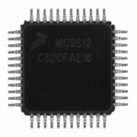
Manufacturer Part Number
MC9S12C32CFAE16
Description
IC MCU 32K FLASH 16MHZ 48-LQFP
Manufacturer
Freescale Semiconductor
Series
HCS12r
Datasheets
1.MC9S12GC16MFUE.pdf
(690 pages)
2.MC9S12C96CFUER.pdf
(26 pages)
3.MC9S12C32CFAE25.pdf
(2 pages)
Specifications of MC9S12C32CFAE16
Core Processor
HCS12
Core Size
16-Bit
Speed
16MHz
Connectivity
CAN, EBI/EMI, SCI, SPI
Peripherals
POR, PWM, WDT
Number Of I /o
31
Program Memory Size
32KB (32K x 8)
Program Memory Type
FLASH
Ram Size
2K x 8
Voltage - Supply (vcc/vdd)
2.35 V ~ 5.5 V
Data Converters
A/D 8x10b
Oscillator Type
Internal
Operating Temperature
-40°C ~ 85°C
Package / Case
48-LQFP
Cpu Family
HCS12
Device Core Size
16b
Frequency (max)
16MHz
Interface Type
CAN/SCI/SPI
Total Internal Ram Size
2KB
# I/os (max)
31
Number Of Timers - General Purpose
8
Operating Supply Voltage (typ)
2.5/5V
Operating Supply Voltage (max)
2.75/5.5V
Operating Supply Voltage (min)
2.35/2.97V
On-chip Adc
8-chx10-bit
Instruction Set Architecture
CISC
Operating Temp Range
-40C to 85C
Operating Temperature Classification
Industrial
Mounting
Surface Mount
Pin Count
48
Package Type
LQFP
Package
48LQFP
Family Name
HCS12
Maximum Speed
16 MHz
Operating Supply Voltage
2.5|5 V
Data Bus Width
16 Bit
Number Of Programmable I/os
31
Number Of Timers
8
For Use With
CML12C32SLK - KIT STUDENT LEARNING 16BIT HCS12
Lead Free Status / RoHS Status
Lead free / RoHS Compliant
Eeprom Size
-
Lead Free Status / Rohs Status
Compliant
Available stocks
Company
Part Number
Manufacturer
Quantity
Price

Company:
Part Number:
MC9S12C32CFAE16
Manufacturer:
Freescale Semiconductor
Quantity:
10 000


Read: anytime
Write: anytime
12.3.2.14 PWM Channel Duty Registers (PWMDTYx)
There is a dedicated duty register for each channel. The value in this register determines the duty of the
associated PWM channel. The duty value is compared to the counter and if it is equal to the counter value
a match occurs and the output changes state.
The duty registers for each channel are double buffered so that if they change while the channel is enabled,
the change will NOT take effect until one of the following occurs:
In this way, the output of the PWM will always be either the old duty waveform or the new duty waveform,
not some variation in between. If the channel is not enabled, then writes to the duty register will go directly
to the latches as well as the buffer.
Freescale Semiconductor
Module Base + 0x0015
Module Base + 0x0016
Module Base + 0x0017
Reset
Reset
Reset
•
•
•
W
W
W
R
R
R
The effective period ends
The counter is written (counter resets to 0x0000)
The channel is disabled
Bit 7
Bit 7
Bit 7
0
0
0
7
7
7
Figure 12-24. PWM Channel Period Registers (PWMPER3)
Figure 12-25. PWM Channel Period Registers (PWMPER4)
Figure 12-26. PWM Channel Period Registers (PWMPER5)
6
0
6
0
6
0
6
6
6
MC9S12C-Family / MC9S12GC-Family
5
0
5
0
5
0
5
5
5
Rev 01.24
4
0
4
0
4
0
4
4
4
Chapter 12 Pulse-Width Modulator (PWM8B6CV1) Block Description
3
0
3
0
3
0
3
3
3
2
0
2
0
2
0
2
2
2
1
0
1
0
1
0
1
1
1
Bit 0
Bit 0
Bit 0
0
0
0
0
0
0
367
Related parts for MC9S12C32CFAE16
Image
Part Number
Description
Manufacturer
Datasheet
Request
R

Part Number:
Description:
Manufacturer:
Freescale Semiconductor, Inc
Datasheet:
Part Number:
Description:
Manufacturer:
Freescale Semiconductor, Inc
Datasheet:
Part Number:
Description:
Manufacturer:
Freescale Semiconductor, Inc
Datasheet:
Part Number:
Description:
Manufacturer:
Freescale Semiconductor, Inc
Datasheet:
Part Number:
Description:
Manufacturer:
Freescale Semiconductor, Inc
Datasheet:
Part Number:
Description:
Manufacturer:
Freescale Semiconductor, Inc
Datasheet:
Part Number:
Description:
Manufacturer:
Freescale Semiconductor, Inc
Datasheet:
Part Number:
Description:
Manufacturer:
Freescale Semiconductor, Inc
Datasheet:
Part Number:
Description:
Manufacturer:
Freescale Semiconductor, Inc
Datasheet:
Part Number:
Description:
Manufacturer:
Freescale Semiconductor, Inc
Datasheet:
Part Number:
Description:
Manufacturer:
Freescale Semiconductor, Inc
Datasheet:
Part Number:
Description:
Manufacturer:
Freescale Semiconductor, Inc
Datasheet:
Part Number:
Description:
Manufacturer:
Freescale Semiconductor, Inc
Datasheet:
Part Number:
Description:
Manufacturer:
Freescale Semiconductor, Inc
Datasheet:
Part Number:
Description:
Manufacturer:
Freescale Semiconductor, Inc
Datasheet: