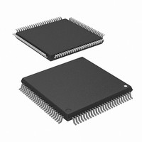
R5F2L3A8ANFP#U1 Renesas Electronics America, R5F2L3A8ANFP#U1 Datasheet - Page 589

R5F2L3A8ANFP#U1
Manufacturer Part Number
R5F2L3A8ANFP#U1
Description
MCU 1KB FLASH 64K ROM 100-LQFP
Manufacturer
Renesas Electronics America
Series
R8C/Lx/3AAr
Datasheet
1.R5F2L387ANFPU1.pdf
(864 pages)
Specifications of R5F2L3A8ANFP#U1
Core Processor
R8C
Core Size
16/32-Bit
Speed
20MHz
Connectivity
I²C, LIN, SIO, SSU, UART/USART
Peripherals
LCD, POR, PWM, Voltage Detect, WDT
Number Of I /o
88
Program Memory Size
64KB (64K x 8)
Program Memory Type
FLASH
Ram Size
8K x 8
Voltage - Supply (vcc/vdd)
1.8 V ~ 5.5 V
Data Converters
A/D 20x10b; D/A 2x8b
Oscillator Type
Internal
Operating Temperature
-20°C ~ 85°C
Package / Case
100-LQFP
Lead Free Status / RoHS Status
Lead free / RoHS Compliant
Eeprom Size
-
Lead Free Status / Rohs Status
Supplier Unconfirmed
Available stocks
Company
Part Number
Manufacturer
Quantity
Price
- Current page: 589 of 864
- Download datasheet (16Mb)
R8C/L35A Group, R8C/L36A Group, R8C/L38A Group, R8C/L3AA Group,
R8C/L35B Group, R8C/L36B Group, R8C/L38B Group, R8C/L3AB Group
REJ09B0441-0100 Rev.1.00
Page 552 of 802
26.2.5
Notes:
26.2.6
Notes:
b15 to b0
1. When the ORER bit in the SSSR register is set to 1 (overrun error), the SSRDR register retains the data received
2. When the SSU data transfer length is set to 9 bits or more with the SSBR register, access the SSRDR register in
1. The set clock is used when an internal clock is selected.
2. The SSCK pin functions as the transfer clock output pin when the MSS bit is set to 1 (operation as the master
3. The RSSTP bit is disabled when the MSS bit is set to 0 (operation as a slave device).
After Reset
After Reset
After Reset
Bit
b0
b1
b2
b3
b4
b5
b6
b7
Bit
Address 0197h to 0196h
Address 0198h
before an overrun error occurs. When an overrun error occurs, the receive data is discarded.
16-bit units.
device). The MSS bit is set to 0 (operation as a slave device) when the CE bit in the SSSR register is set to 1
(conflict error occurs).
Symbol
Symbol
Symbol
Symbol
RSSTP Receive single stop bit
Bit
Bit
Bit
CKS0
CKS1
CKS2
MSS
SS Receive Data Register (SSRDR)
SS Control Register H (SSCRH)
Symbol
—
—
—
—
b15
b7
b7
—
—
—
1
1
0
Transfer clock select bit
Nothing is assigned. If necessary, set to 0. When read, the content is 0.
Master/slave device select bit
Nothing is assigned. If necessary, set to 0. When read, the content is 0.
This register stores receive data.
The receive data is transferred to the SSRDR register and the receive operation is
completed when 1 byte of data has been received by the SSTRSR register. At this time,
the next reception is enabled.
Continuous reception is enabled using registers SSTRSR and SSRDR.
RSSTP
b14
b6
b6
—
—
1
1
0
Oct 30, 2009
Bit Name
MSS
b13
b5
—
—
b5
1
1
0
(3)
(1)
b12
(2)
b4
b4
—
—
—
1
1
0
(1, 2)
b2 b1 b0
0: Operation as a slave device
1: Operation as the master device
0: Receive operation is continued after receiving 1 byte
1: Receive operation is completed after receiving 1
0 0 0: f1/256
0 0 1: f1/128
0 1 0: f1/64
0 1 1: f1/32
1 0 0: f1/16
1 0 1: f1/8
1 1 0: f1/4
1 1 1: Do not set.
of data
byte of data
b11
b3
b3
—
—
—
Function
1
1
0
26. Synchronous Serial Communication Unit (SSU)
CKS2
b10
b2
b2
—
—
1
1
0
Function
CKS1
b1
b9
b1
—
—
1
1
0
CKS0
b0
b8
b0
—
—
1
1
0
R/W
R/W
R/W
R/W
R/W
R/W
R/W
—
—
R
Related parts for R5F2L3A8ANFP#U1
Image
Part Number
Description
Manufacturer
Datasheet
Request
R

Part Number:
Description:
KIT STARTER FOR M16C/29
Manufacturer:
Renesas Electronics America
Datasheet:

Part Number:
Description:
KIT STARTER FOR R8C/2D
Manufacturer:
Renesas Electronics America
Datasheet:

Part Number:
Description:
R0K33062P STARTER KIT
Manufacturer:
Renesas Electronics America
Datasheet:

Part Number:
Description:
KIT STARTER FOR R8C/23 E8A
Manufacturer:
Renesas Electronics America
Datasheet:

Part Number:
Description:
KIT STARTER FOR R8C/25
Manufacturer:
Renesas Electronics America
Datasheet:

Part Number:
Description:
KIT STARTER H8S2456 SHARPE DSPLY
Manufacturer:
Renesas Electronics America
Datasheet:

Part Number:
Description:
KIT STARTER FOR R8C38C
Manufacturer:
Renesas Electronics America
Datasheet:

Part Number:
Description:
KIT STARTER FOR R8C35C
Manufacturer:
Renesas Electronics America
Datasheet:

Part Number:
Description:
KIT STARTER FOR R8CL3AC+LCD APPS
Manufacturer:
Renesas Electronics America
Datasheet:

Part Number:
Description:
KIT STARTER FOR RX610
Manufacturer:
Renesas Electronics America
Datasheet:

Part Number:
Description:
KIT STARTER FOR R32C/118
Manufacturer:
Renesas Electronics America
Datasheet:

Part Number:
Description:
KIT DEV RSK-R8C/26-29
Manufacturer:
Renesas Electronics America
Datasheet:

Part Number:
Description:
KIT STARTER FOR SH7124
Manufacturer:
Renesas Electronics America
Datasheet:

Part Number:
Description:
KIT STARTER FOR H8SX/1622
Manufacturer:
Renesas Electronics America
Datasheet:

Part Number:
Description:
KIT DEV FOR SH7203
Manufacturer:
Renesas Electronics America
Datasheet:


