R5F2L3A8ANFP#U1 Renesas Electronics America, R5F2L3A8ANFP#U1 Datasheet - Page 214
R5F2L3A8ANFP#U1
Manufacturer Part Number
R5F2L3A8ANFP#U1
Description
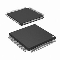
MCU 1KB FLASH 64K ROM 100-LQFP
Manufacturer
Renesas Electronics America
Series
R8C/Lx/3AAr
Datasheet
1.R5F2L387ANFPU1.pdf
(864 pages)
Specifications of R5F2L3A8ANFP#U1
Core Processor
R8C
Core Size
16/32-Bit
Speed
20MHz
Connectivity
I²C, LIN, SIO, SSU, UART/USART
Peripherals
LCD, POR, PWM, Voltage Detect, WDT
Number Of I /o
88
Program Memory Size
64KB (64K x 8)
Program Memory Type
FLASH
Ram Size
8K x 8
Voltage - Supply (vcc/vdd)
1.8 V ~ 5.5 V
Data Converters
A/D 20x10b; D/A 2x8b
Oscillator Type
Internal
Operating Temperature
-20°C ~ 85°C
Package / Case
100-LQFP
Lead Free Status / RoHS Status
Lead free / RoHS Compliant
Eeprom Size
-
Lead Free Status / Rohs Status
Supplier Unconfirmed
Available stocks
Company
Part Number
Manufacturer
Quantity
Price


R8C/L35A Group, R8C/L36A Group, R8C/L38A Group, R8C/L3AA Group,
R8C/L35B Group, R8C/L36B Group, R8C/L38B Group, R8C/L3AB Group
REJ09B0441-0100 Rev.1.00
Page 177 of 802
As with other maskable interrupts, the interrupts of timer RC, timer RD (timer RD0), timer RD (timer RD1), timer
RG, the synchronous serial communication unit, the I
combination of the I flag, IR bit, bits ILVL0 to ILVL2, and IPL. However, since each interrupt source is generated
by a combination of multiple interrupt request sources, the following differences from other maskable interrupts
apply:
•
•
•
•
•
Refer to chapters of the individual peripheral functions (19. Timer RC, 20. Timer RD, 22. Timer RG, 26.
Synchronous Serial Communication Unit (SSU), 27. I
register and enable register.
For the interrupt control register, refer to 11.3 Interrupt Control.
When bits in the enable register are set to 1 and the corresponding bits in the status register are set to 1 (interrupt
enabled), the IR bit in the interrupt control register is set to 1 (interrupt requested).
When either bits in the status register or the corresponding bits in the enable register, or both are set to 0, the IR
bit is set to 0 (no interrupt requested).
That is, even if the interrupt is not acknowledged after the IR bit is set to 1, the interrupt request will not be
retained.
Also, the IR bit is not set to 0 even if 0 is written to this bit.
Individual bits in the status register are not automatically set to 0 even if the interrupt is acknowledged.
The IR bit is also not automatically set to 0 when the interrupt is acknowledged.
Set individual bits in the status register to 0 in the interrupt routine. Refer to the status register figure for how to
set individual bits in the status register to 0.
When multiple bits in the enable register are set to 1 and other request sources are generated after the IR bit is set
to 1, the IR bit remains 1.
When multiple bits in the enable register are set to 1, use the status register to determine which request source
causes an interrupt.
Oct 30, 2009
2
C bus interface, and the flash memory are controlled by the
2
C bus Interface, and 33. Flash Memory) for the status
11. Interrupts
Related parts for R5F2L3A8ANFP#U1
Image
Part Number
Description
Manufacturer
Datasheet
Request
R

Part Number:
Description:
KIT STARTER FOR M16C/29
Manufacturer:
Renesas Electronics America
Datasheet:

Part Number:
Description:
KIT STARTER FOR R8C/2D
Manufacturer:
Renesas Electronics America
Datasheet:

Part Number:
Description:
R0K33062P STARTER KIT
Manufacturer:
Renesas Electronics America
Datasheet:

Part Number:
Description:
KIT STARTER FOR R8C/23 E8A
Manufacturer:
Renesas Electronics America
Datasheet:

Part Number:
Description:
KIT STARTER FOR R8C/25
Manufacturer:
Renesas Electronics America
Datasheet:

Part Number:
Description:
KIT STARTER H8S2456 SHARPE DSPLY
Manufacturer:
Renesas Electronics America
Datasheet:

Part Number:
Description:
KIT STARTER FOR R8C38C
Manufacturer:
Renesas Electronics America
Datasheet:

Part Number:
Description:
KIT STARTER FOR R8C35C
Manufacturer:
Renesas Electronics America
Datasheet:

Part Number:
Description:
KIT STARTER FOR R8CL3AC+LCD APPS
Manufacturer:
Renesas Electronics America
Datasheet:
Part Number:
Description:
KIT STARTER FOR RX610
Manufacturer:
Renesas Electronics America
Datasheet:

Part Number:
Description:
KIT STARTER FOR R32C/118
Manufacturer:
Renesas Electronics America
Datasheet:

Part Number:
Description:
KIT DEV RSK-R8C/26-29
Manufacturer:
Renesas Electronics America
Datasheet:

Part Number:
Description:
KIT STARTER FOR SH7124
Manufacturer:
Renesas Electronics America
Datasheet:

Part Number:
Description:
KIT STARTER FOR H8SX/1622
Manufacturer:
Renesas Electronics America
Datasheet:

Part Number:
Description:
KIT DEV FOR SH7203
Manufacturer:
Renesas Electronics America
Datasheet: