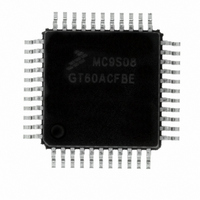
MC9S08GT60ACFBE Freescale Semiconductor, MC9S08GT60ACFBE Datasheet - Page 191

MC9S08GT60ACFBE
Manufacturer Part Number
MC9S08GT60ACFBE
Description
IC MCU 60K FLASH 4K RAM 44-QFP
Manufacturer
Freescale Semiconductor
Series
HCS08r
Datasheet
1.MC9S08GT60ACFDER.pdf
(302 pages)
Specifications of MC9S08GT60ACFBE
Core Processor
HCS08
Core Size
8-Bit
Speed
40MHz
Connectivity
I²C, SCI, SPI
Peripherals
LVD, POR, PWM, WDT
Number Of I /o
36
Program Memory Size
60KB (60K x 8)
Program Memory Type
FLASH
Ram Size
4K x 8
Voltage - Supply (vcc/vdd)
1.8 V ~ 3.6 V
Data Converters
A/D 8x10b
Oscillator Type
Internal
Operating Temperature
-40°C ~ 85°C
Package / Case
44-QFP
Cpu Family
HCS08
Device Core Size
8b
Frequency (max)
40MHz
Interface Type
I2C/SCI/SPI
Total Internal Ram Size
4KB
# I/os (max)
36
Number Of Timers - General Purpose
4
Operating Supply Voltage (typ)
2.5/3.3V
Operating Supply Voltage (max)
3.6V
Operating Supply Voltage (min)
1.8/2.08V
On-chip Adc
8-chx10-bit
Instruction Set Architecture
CISC
Operating Temp Range
-40C to 85C
Operating Temperature Classification
Industrial
Mounting
Surface Mount
Pin Count
44
Package Type
PQFP
Processor Series
S08GT
Core
HCS08
Data Bus Width
8 bit
Data Ram Size
4 KB
Maximum Clock Frequency
20 MHz
Number Of Programmable I/os
39
Number Of Timers
2
Operating Supply Voltage
0 V to 1.8 V
Maximum Operating Temperature
+ 85 C
Mounting Style
SMD/SMT
3rd Party Development Tools
EWS08
Development Tools By Supplier
M68EVB908GB60E, M68DEMO908GB60E
Minimum Operating Temperature
- 40 C
For Use With
M68DEMO908GB60E - BOARD DEMO MC9S08GB60M68EVB908GB60E - BOARD EVAL FOR MC9S08GB60
Lead Free Status / RoHS Status
Lead free / RoHS Compliant
Eeprom Size
-
Lead Free Status / Rohs Status
Compliant
Available stocks
Company
Part Number
Manufacturer
Quantity
Price
Company:
Part Number:
MC9S08GT60ACFBE
Manufacturer:
Freescale Semiconductor
Quantity:
10 000
Part Number:
MC9S08GT60ACFBE
Manufacturer:
FREESCALE深圳进口
Quantity:
20 000
Company:
Part Number:
MC9S08GT60ACFBER
Manufacturer:
Freescale Semiconductor
Quantity:
10 000
- Current page: 191 of 302
- Download datasheet (8Mb)
12.1.1
Features of the SPI module include:
12.1.2
This section includes block diagrams showing SPI system connections, the internal organization of the SPI
module, and the SPI clock dividers that control the master mode bit rate.
12.1.2.1
Figure 12-2
device initiates all SPI data transfers. During a transfer, the master shifts data out (on the MOSI pin) to the
slave while simultaneously shifting data in (on the MISO pin) from the slave. The transfer effectively
exchanges the data that was in the SPI shift registers of the two SPI systems. The SPSCK signal is a clock
output from the master and an input to the slave. The slave device must be selected by a low level on the
slave select input (SS pin). In this system, the master device has configured its SS pin as an optional slave
select output.
Freescale Semiconductor
•
•
•
•
•
•
•
Master or slave mode operation
Full-duplex or single-wire bidirectional option
Programmable transmit bit rate
Double-buffered transmit and receive
Serial clock phase and polarity options
Slave select output
Selectable MSB-first or LSB-first shifting
7
6
Features
Block Diagrams
shows the SPI modules of two MCUs connected in a master-slave arrangement. The master
SPI System Block Diagram
5
GENERATOR
SPI SHIFTER
MASTER
CLOCK
4
3
2
1
0
Figure 12-2. SPI System Connections
MC9S08GB60A Data Sheet, Rev. 2
MOSI
MISO
SPSCK
SS
SPSCK
MOSI
MISO
SS
7
SLAVE
6
5
SPI SHIFTER
4
Serial Peripheral Interface (S08SPIV3)
3
2
1
0
191
Related parts for MC9S08GT60ACFBE
Image
Part Number
Description
Manufacturer
Datasheet
Request
R
Part Number:
Description:
Manufacturer:
Freescale Semiconductor, Inc
Datasheet:
Part Number:
Description:
Manufacturer:
Freescale Semiconductor, Inc
Datasheet:
Part Number:
Description:
Manufacturer:
Freescale Semiconductor, Inc
Datasheet:
Part Number:
Description:
Manufacturer:
Freescale Semiconductor, Inc
Datasheet:
Part Number:
Description:
Manufacturer:
Freescale Semiconductor, Inc
Datasheet:
Part Number:
Description:
Manufacturer:
Freescale Semiconductor, Inc
Datasheet:
Part Number:
Description:
Manufacturer:
Freescale Semiconductor, Inc
Datasheet:
Part Number:
Description:
Manufacturer:
Freescale Semiconductor, Inc
Datasheet:
Part Number:
Description:
Manufacturer:
Freescale Semiconductor, Inc
Datasheet:
Part Number:
Description:
Manufacturer:
Freescale Semiconductor, Inc
Datasheet:
Part Number:
Description:
Manufacturer:
Freescale Semiconductor, Inc
Datasheet:
Part Number:
Description:
Manufacturer:
Freescale Semiconductor, Inc
Datasheet:
Part Number:
Description:
Manufacturer:
Freescale Semiconductor, Inc
Datasheet:
Part Number:
Description:
Manufacturer:
Freescale Semiconductor, Inc
Datasheet:
Part Number:
Description:
Manufacturer:
Freescale Semiconductor, Inc
Datasheet:


