MC908GP16CBE Freescale Semiconductor, MC908GP16CBE Datasheet - Page 42
MC908GP16CBE
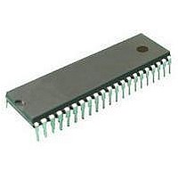
Manufacturer Part Number
MC908GP16CBE
Description
IC MCU 16K FLASH 42-SDIP
Manufacturer
Freescale Semiconductor
Series
HC08r
Datasheet
1.MC908GP32CFBE.pdf
(266 pages)
Specifications of MC908GP16CBE
Core Processor
HC08
Core Size
8-Bit
Speed
8MHz
Connectivity
SCI, SPI
Peripherals
LVD, POR, PWM
Number Of I /o
31
Program Memory Size
16KB (16K x 8)
Program Memory Type
FLASH
Ram Size
512 x 8
Voltage - Supply (vcc/vdd)
2.7 V ~ 5.5 V
Data Converters
A/D 8x8b
Oscillator Type
Internal
Operating Temperature
-40°C ~ 85°C
Package / Case
42-DIP (0.600", 15.24mm)
Processor Series
HC08GP
Core
HC08
Data Bus Width
8 bit
Data Ram Size
512 B
Interface Type
SCI, SPI
Maximum Clock Frequency
8.2 MHz
Number Of Programmable I/os
33
Number Of Timers
4
Maximum Operating Temperature
+ 85 C
Mounting Style
Through Hole
Development Tools By Supplier
FSICEBASE, DEMO908GZ60E, M68CBL05CE, M68EML08GPGTE
Minimum Operating Temperature
- 40 C
On-chip Adc
8 bit, 8 Channel
Lead Free Status / RoHS Status
Lead free / RoHS Compliant
Eeprom Size
-
Lead Free Status / Rohs Status
Details
Available stocks
Company
Part Number
Manufacturer
Quantity
Price

Part Number:
MC908GP16CBE
Manufacturer:
FREESCALE
Quantity:
20 000


Memory
2.6.6 FLASH Block Protection
Due to the ability of the on-board charge pump to erase and program the FLASH memory in the target
application, provision is made for protecting a block of memory from unintentional erase or program
operations due to system malfunction. This protection is done by using of a FLASH Block Protect Register
(FLBPR). The FLBPR determines the range of the FLASH memory which is to be protected. The range
of the protected area starts from a location defined by FLBPR and ends at the bottom of the FLASH
memory ($FFFF). When the memory is protected, the HVEN bit cannot be set in either ERASE or
PROGRAM operations.
42
PGM bit (step 7 to step 10) must not exceed the maximum programming
time, t
Be cautious when programming the FLASH array to ensure that
non-FLASH locations are not used as the address that is written to when
selecting either the desired row address range in step 3 of the algorithm or
the byte to be programmed in step 7 of the algorithm. This applies
particularly to $FFD4–$FFDF.
In performing a program or erase operation, the FLASH block protect
register must be read after setting the PGM or ERASE bit and before
asserting the HVEN bit
PROG
maximum.
MC68HC908GP32 Data Sheet, Rev. 10
NOTE
NOTE
Freescale Semiconductor
Related parts for MC908GP16CBE
Image
Part Number
Description
Manufacturer
Datasheet
Request
R

Part Number:
Description:
Manufacturer:
Freescale Semiconductor, Inc
Datasheet:
Part Number:
Description:
Manufacturer:
Freescale Semiconductor, Inc
Datasheet:
Part Number:
Description:
Manufacturer:
Freescale Semiconductor, Inc
Datasheet:
Part Number:
Description:
Manufacturer:
Freescale Semiconductor, Inc
Datasheet:
Part Number:
Description:
Manufacturer:
Freescale Semiconductor, Inc
Datasheet:
Part Number:
Description:
Manufacturer:
Freescale Semiconductor, Inc
Datasheet:
Part Number:
Description:
Manufacturer:
Freescale Semiconductor, Inc
Datasheet:
Part Number:
Description:
Manufacturer:
Freescale Semiconductor, Inc
Datasheet:
Part Number:
Description:
Manufacturer:
Freescale Semiconductor, Inc
Datasheet:
Part Number:
Description:
Manufacturer:
Freescale Semiconductor, Inc
Datasheet:
Part Number:
Description:
Manufacturer:
Freescale Semiconductor, Inc
Datasheet:
Part Number:
Description:
Manufacturer:
Freescale Semiconductor, Inc
Datasheet:
Part Number:
Description:
Manufacturer:
Freescale Semiconductor, Inc
Datasheet:
Part Number:
Description:
Manufacturer:
Freescale Semiconductor, Inc
Datasheet:
Part Number:
Description:
Manufacturer:
Freescale Semiconductor, Inc
Datasheet: