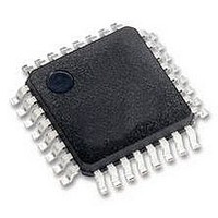
MCHC908GR8AMFAER Freescale Semiconductor, MCHC908GR8AMFAER Datasheet - Page 223

MCHC908GR8AMFAER
Manufacturer Part Number
MCHC908GR8AMFAER
Description
IC MCU 8K FLASH 8MHZ 32-LQFP
Manufacturer
Freescale Semiconductor
Series
HC08r
Specifications of MCHC908GR8AMFAER
Core Processor
HC08
Core Size
8-Bit
Speed
8MHz
Connectivity
SCI, SPI
Peripherals
LVD, POR, PWM
Number Of I /o
21
Program Memory Size
7.5KB (7.5K x 8)
Program Memory Type
FLASH
Ram Size
384 x 8
Voltage - Supply (vcc/vdd)
2.7 V ~ 5.5 V
Data Converters
A/D 6x8b
Oscillator Type
Internal
Operating Temperature
-40°C ~ 125°C
Package / Case
32-LQFP
Controller Family/series
HC08
No. Of I/o's
21
Ram Memory Size
384Byte
Cpu Speed
8MHz
No. Of Timers
2
Embedded Interface Type
I2C, SCI, SPI
Rohs Compliant
Yes
Processor Series
HC08G
Core
HC08
Data Bus Width
8 bit
Data Ram Size
384 B
Interface Type
SCI, SPI
Maximum Clock Frequency
8.2 MHz
Number Of Programmable I/os
21
Number Of Timers
3
Maximum Operating Temperature
+ 125 C
Mounting Style
SMD/SMT
Development Tools By Supplier
FSICEBASE, DEMO908GZ60E, M68CBL05CE, M68EML08GPGTE
Minimum Operating Temperature
- 40 C
On-chip Adc
8 bit, 6 Channel
Lead Free Status / RoHS Status
Lead free / RoHS Compliant
Eeprom Size
-
Lead Free Status / Rohs Status
Details
Available stocks
Company
Part Number
Manufacturer
Quantity
Price
Company:
Part Number:
MCHC908GR8AMFAER
Manufacturer:
Freescale Semiconductor
Quantity:
10 000
- Current page: 223 of 292
- Download datasheet (4Mb)
18.2 Features
Features of the TIM include:
18.3 Pin Name Conventions
The text that follows describes both timers, TIM1 and TIM2. The TIM input/output (I/O) pin names are
T[1,2]CH0 (timer channel 0) and T[1,2]CH1 (timer channel 1), where “1” is used to indicate TIM1 and “2”
is used to indicate TIM2. The two TIMs share four I/O pins with four port D I/O port pins.
18.4 Functional Description
Figure 18-1
that can operate as a free-running counter or a modulo up-counter. The TIM counter provides the timing
reference for the input capture and output compare functions. The TIM counter modulo registers,
TMODH:TMODL, control the modulo value of the TIM counter. Software can read the TIM counter value
at any time without affecting the counting sequence.
The two TIM channels (per timer) are programmable independently as input capture or output compare
channels. If a channel is configured as input capture, then an internal pullup device may be enabled for
that channel. See
Figure 18-3
Freescale Semiconductor
•
•
•
•
•
•
Two input capture/output compare channels:
–
–
Buffered and unbuffered pulse-width-modulation (PWM) signal generation
Programmable TIM clock input with 7-frequency internal bus clock prescaler selection
Free-running or modulo up-count operation
Toggle any channel pin on overflow
TIM counter stop and reset bits
Rising-edge, falling-edge, or any-edge input capture trigger
Set, clear, or toggle output compare action
shows the structure of the TIM. The central component of the TIM is the 16-bit TIM counter
summarizes the timer registers.
References to either timer 1 or timer 2 may be made in the following text by
omitting the timer number. For example, TCH0 may refer generically to
T1CH0 and T2CH0, and TCH1 may refer to T1CH1 and T2CH1.
References to either timer 1 or timer 2 may be made in the following text by
omitting the timer number. For example, TSC may generically refer to both
T1SC and T2SC.
12.5.3 Port D Input Pullup Enable Register.
MC68HC908GT16 • MC68HC908GT8 • MC68HC08GT16 Data Sheet, Rev. 5.0
NOTE
NOTE
Features
223
Related parts for MCHC908GR8AMFAER
Image
Part Number
Description
Manufacturer
Datasheet
Request
R
Part Number:
Description:
Manufacturer:
Freescale Semiconductor, Inc
Datasheet:
Part Number:
Description:
Manufacturer:
Freescale Semiconductor, Inc
Datasheet:
Part Number:
Description:
Manufacturer:
Freescale Semiconductor, Inc
Datasheet:
Part Number:
Description:
Manufacturer:
Freescale Semiconductor, Inc
Datasheet:
Part Number:
Description:
Manufacturer:
Freescale Semiconductor, Inc
Datasheet:
Part Number:
Description:
Manufacturer:
Freescale Semiconductor, Inc
Datasheet:
Part Number:
Description:
Manufacturer:
Freescale Semiconductor, Inc
Datasheet:
Part Number:
Description:
Manufacturer:
Freescale Semiconductor, Inc
Datasheet:
Part Number:
Description:
Manufacturer:
Freescale Semiconductor, Inc
Datasheet:
Part Number:
Description:
Manufacturer:
Freescale Semiconductor, Inc
Datasheet:
Part Number:
Description:
Manufacturer:
Freescale Semiconductor, Inc
Datasheet:
Part Number:
Description:
Manufacturer:
Freescale Semiconductor, Inc
Datasheet:
Part Number:
Description:
Manufacturer:
Freescale Semiconductor, Inc
Datasheet:
Part Number:
Description:
Manufacturer:
Freescale Semiconductor, Inc
Datasheet:
Part Number:
Description:
Manufacturer:
Freescale Semiconductor, Inc
Datasheet:


