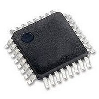
MCHC908GR8AMFAER Freescale Semiconductor, MCHC908GR8AMFAER Datasheet - Page 22

MCHC908GR8AMFAER
Manufacturer Part Number
MCHC908GR8AMFAER
Description
IC MCU 8K FLASH 8MHZ 32-LQFP
Manufacturer
Freescale Semiconductor
Series
HC08r
Specifications of MCHC908GR8AMFAER
Core Processor
HC08
Core Size
8-Bit
Speed
8MHz
Connectivity
SCI, SPI
Peripherals
LVD, POR, PWM
Number Of I /o
21
Program Memory Size
7.5KB (7.5K x 8)
Program Memory Type
FLASH
Ram Size
384 x 8
Voltage - Supply (vcc/vdd)
2.7 V ~ 5.5 V
Data Converters
A/D 6x8b
Oscillator Type
Internal
Operating Temperature
-40°C ~ 125°C
Package / Case
32-LQFP
Controller Family/series
HC08
No. Of I/o's
21
Ram Memory Size
384Byte
Cpu Speed
8MHz
No. Of Timers
2
Embedded Interface Type
I2C, SCI, SPI
Rohs Compliant
Yes
Processor Series
HC08G
Core
HC08
Data Bus Width
8 bit
Data Ram Size
384 B
Interface Type
SCI, SPI
Maximum Clock Frequency
8.2 MHz
Number Of Programmable I/os
21
Number Of Timers
3
Maximum Operating Temperature
+ 125 C
Mounting Style
SMD/SMT
Development Tools By Supplier
FSICEBASE, DEMO908GZ60E, M68CBL05CE, M68EML08GPGTE
Minimum Operating Temperature
- 40 C
On-chip Adc
8 bit, 6 Channel
Lead Free Status / RoHS Status
Lead free / RoHS Compliant
Eeprom Size
-
Lead Free Status / Rohs Status
Details
Available stocks
Company
Part Number
Manufacturer
Quantity
Price
Company:
Part Number:
MCHC908GR8AMFAER
Manufacturer:
Freescale Semiconductor
Quantity:
10 000
- Current page: 22 of 292
- Download datasheet (4Mb)
General Description
22
•
•
•
•
•
•
•
•
•
•
•
•
•
•
•
•
•
•
•
•
•
•
•
System protection features:
–
–
–
–
Low-power design; fully static with stop and wait modes
Standard low-power modes of operation:
–
–
Master reset pin and power-on reset (POR)
16 Kbytes of on-chip 100k cycle write/erase capable Flash memory (8 Kbytes on
MC68HC908GT8)
512 bytes of on-chip random-access memory (RAM)
720 bytes of Flash programming routines ROM
Serial peripheral interface module (SPI)
Serial communications interface module (SCI)
Two 16-bit, 2-channel timer interface modules (TIM1 and TIM2) with selectable input capture,
output compare, and pulse-width modulation (PWM) capability on each channel
8-channel, 8-bit successive approximation analog-to-digital converter (ADC)
Break module (BRK) to allow single breakpoint setting during in-circuit debugging
Internal pullups on IRQ and RST to reduce customer system cost
Up to 36 general-purpose input/output (I/O) pins, including:
–
–
Selectable pullups on inputs only on ports A, C, and D. Selection is on an individual port bit basis.
During output mode, pullups are disengaged.
High current 10-mA sink/10-mA source capability on all port pins
Higher current 20-mA sink/source capability on PTC0–PTC4
Timebase module with clock prescaler circuitry for eight user selectable periodic real-time
interrupts with optional active clock source during stop mode for periodic wakeup from stop using
an external 32-kHz crystal or internal oscillator
User selection of having the oscillator enabled or disabled during stop mode
8-bit keyboard wakeup port
Available packages:
–
–
Specific features of the MC68HC908GT16 in 42-pin SDIP are:
–
–
Specific features of the MC68HC908GT16 in 44-pin QFP are:
–
–
Optional computer operating properly (COP) reset
Low-voltage detection with optional reset and selectable trip points for 3.0-V and 5.0-V
operation
Illegal opcode detection with reset
Illegal address detection with reset
Wait mode
Stop mode
28 shared-function I/O pins
Six or eight dedicated I/O pins, depending on package choice
42-pin shrink dual in-line package (SDIP)
44-pin quad flat pack (QFP)
Port C is only 5 bits: PTC0–PTC4
Port D is 8 bits: PTD0–PTD7; dual 2-channel TIM modules
Port C is 7 bits: PTC0–PTC6
Port D is 8 bits: PTD0–PTD7; dual 2-channel TIM modules
MC68HC908GT16 • MC68HC908GT8 • MC68HC08GT16 Data Sheet, Rev. 5.0
Freescale Semiconductor
Related parts for MCHC908GR8AMFAER
Image
Part Number
Description
Manufacturer
Datasheet
Request
R
Part Number:
Description:
Manufacturer:
Freescale Semiconductor, Inc
Datasheet:
Part Number:
Description:
Manufacturer:
Freescale Semiconductor, Inc
Datasheet:
Part Number:
Description:
Manufacturer:
Freescale Semiconductor, Inc
Datasheet:
Part Number:
Description:
Manufacturer:
Freescale Semiconductor, Inc
Datasheet:
Part Number:
Description:
Manufacturer:
Freescale Semiconductor, Inc
Datasheet:
Part Number:
Description:
Manufacturer:
Freescale Semiconductor, Inc
Datasheet:
Part Number:
Description:
Manufacturer:
Freescale Semiconductor, Inc
Datasheet:
Part Number:
Description:
Manufacturer:
Freescale Semiconductor, Inc
Datasheet:
Part Number:
Description:
Manufacturer:
Freescale Semiconductor, Inc
Datasheet:
Part Number:
Description:
Manufacturer:
Freescale Semiconductor, Inc
Datasheet:
Part Number:
Description:
Manufacturer:
Freescale Semiconductor, Inc
Datasheet:
Part Number:
Description:
Manufacturer:
Freescale Semiconductor, Inc
Datasheet:
Part Number:
Description:
Manufacturer:
Freescale Semiconductor, Inc
Datasheet:
Part Number:
Description:
Manufacturer:
Freescale Semiconductor, Inc
Datasheet:
Part Number:
Description:
Manufacturer:
Freescale Semiconductor, Inc
Datasheet:


