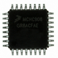
MCHC908GR8ACFAE Freescale Semiconductor, MCHC908GR8ACFAE Datasheet - Page 45

MCHC908GR8ACFAE
Manufacturer Part Number
MCHC908GR8ACFAE
Description
IC MCU 8K FLASH 8MHZ 32-LQFP
Manufacturer
Freescale Semiconductor
Series
HC08r
Specifications of MCHC908GR8ACFAE
Core Processor
HC08
Core Size
8-Bit
Speed
8MHz
Connectivity
SCI, SPI
Peripherals
LVD, POR, PWM
Number Of I /o
21
Program Memory Size
7.5KB (7.5K x 8)
Program Memory Type
FLASH
Ram Size
384 x 8
Voltage - Supply (vcc/vdd)
2.7 V ~ 5.5 V
Data Converters
A/D 6x8b
Oscillator Type
Internal
Operating Temperature
-40°C ~ 85°C
Package / Case
32-LQFP
Controller Family/series
HC08
No. Of I/o's
21
Ram Memory Size
384Byte
Cpu Speed
8MHz
No. Of Timers
2
Embedded Interface Type
I2C, SCI, SPI
Rohs Compliant
Yes
Processor Series
HC08G
Core
HC08
Data Bus Width
8 bit
Data Ram Size
384 B
Interface Type
SCI, SPI
Maximum Clock Frequency
8.2 MHz
Number Of Programmable I/os
21
Number Of Timers
3
Maximum Operating Temperature
+ 85 C
Mounting Style
SMD/SMT
Development Tools By Supplier
FSICEBASE, DEMO908GZ60E, M68CBL05CE, M68EML08GPGTE
Minimum Operating Temperature
- 40 C
On-chip Adc
8 bit, 6 Channel
Lead Free Status / RoHS Status
Lead free / RoHS Compliant
Eeprom Size
-
Lead Free Status / Rohs Status
Details
Available stocks
Company
Part Number
Manufacturer
Quantity
Price
Company:
Part Number:
MCHC908GR8ACFAE
Manufacturer:
Freescale Semiconductor
Quantity:
10 000
- Current page: 45 of 292
- Download datasheet (4Mb)
2.6.6 Flash Block Protection
Due to the ability of the on-board charge pump to erase and program the Flash memory in the target
application, provision is made for protecting a block of memory from unintentional erase or program
operations due to system malfunction. This protection is done by using of a Flash block protect register
(FLBPR). The FLBPR determines the range of the Flash memory which is to be protected. The range of
the protected area starts from a location defined by FLBPR and ends at the bottom of the Flash memory
($FFFF). When the memory is protected, the HVEN bit cannot be set in either ERASE or PROGRAM
operations.
When the FLBPR is program with all 0’s, the entire memory is protected from being programmed and
erased. When all the bits are erased (all 1’s), the entire memory is accessible for program and erase.
When bits within the FLBPR are programmed, they lock a block of memory, address ranges as shown in
2.6.7 Flash Block Protect
any erase or program of the FLBPR or the protected block of Flash memory is prohibited. Mass erase is
disabled whenever any block is protected (FLBPR does not equal $FF). The FLBPR itself can be erased
or programmed only with an external voltage, V
from reset into the monitor mode.
2.6.7 Flash Block Protect Register
The Flash block protect register (FLBPR) is implemented as a byte within the Flash memory, and
therefore can only be written during a programming sequence of the Flash memory. The value in this
register determines the starting location of the protected range within the Flash memory.
BPR[7:0] — Flash Block Protect Bits
Freescale Semiconductor
These eight bits represent bits [13:6] of a 16-bit memory address. Bit 15 and Bit 14 are 1s and bits [5:0]
are 0s.
The resultant 16-bit address is used for specifying the start address of the Flash memory for block
protection. The Flash is protected from this start address to the end of Flash memory, at $FFFF. With
this mechanism, the protect start address can be $XX00, $XX40, $XX80, and $XXC0 (64 bytes page
boundaries) within the Flash memory.
Address:
In performing a program or erase operation, the Flash block protect register
must be read after setting the PGM or ERASE bit and before asserting the
HVEN bit
Reset:
Read:
Write:
MC68HC908GT16 • MC68HC908GT8 • MC68HC08GT16 Data Sheet, Rev. 5.0
START ADDRESS OF FLASH
Write to this register is by a programming sequence to the Flash memory.
$FF7E
BPR7
Bit 7
Register. Once the FLBPR is programmed with a value other than $FF or $FE,
Figure 2-5. Flash Block Protect Register (FLBPR)
BLOCK PROTECT
Figure 2-6. Flash Block Protect Start Address
BPR6
6
Unaffected by reset. Initial value from factory is 1.
1
BPR5
5
1
TST
NOTE
, present on the IRQ pin. This voltage also allows entry
BPR4
FLBPR VALUE
4
16-BIT MEMORY ADDRESS
BPR3
3
BPR2
0 0 0 0 0 0
2
BPR1
1
BPR0
Bit 0
Flash Memory
45
Related parts for MCHC908GR8ACFAE
Image
Part Number
Description
Manufacturer
Datasheet
Request
R
Part Number:
Description:
Manufacturer:
Freescale Semiconductor, Inc
Datasheet:
Part Number:
Description:
Manufacturer:
Freescale Semiconductor, Inc
Datasheet:
Part Number:
Description:
Manufacturer:
Freescale Semiconductor, Inc
Datasheet:
Part Number:
Description:
Manufacturer:
Freescale Semiconductor, Inc
Datasheet:
Part Number:
Description:
Manufacturer:
Freescale Semiconductor, Inc
Datasheet:
Part Number:
Description:
Manufacturer:
Freescale Semiconductor, Inc
Datasheet:
Part Number:
Description:
Manufacturer:
Freescale Semiconductor, Inc
Datasheet:
Part Number:
Description:
Manufacturer:
Freescale Semiconductor, Inc
Datasheet:
Part Number:
Description:
Manufacturer:
Freescale Semiconductor, Inc
Datasheet:
Part Number:
Description:
Manufacturer:
Freescale Semiconductor, Inc
Datasheet:
Part Number:
Description:
Manufacturer:
Freescale Semiconductor, Inc
Datasheet:
Part Number:
Description:
Manufacturer:
Freescale Semiconductor, Inc
Datasheet:
Part Number:
Description:
Manufacturer:
Freescale Semiconductor, Inc
Datasheet:
Part Number:
Description:
Manufacturer:
Freescale Semiconductor, Inc
Datasheet:
Part Number:
Description:
Manufacturer:
Freescale Semiconductor, Inc
Datasheet:


