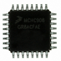
MCHC908GR8ACFAE Freescale Semiconductor, MCHC908GR8ACFAE Datasheet - Page 258

MCHC908GR8ACFAE
Manufacturer Part Number
MCHC908GR8ACFAE
Description
IC MCU 8K FLASH 8MHZ 32-LQFP
Manufacturer
Freescale Semiconductor
Series
HC08r
Specifications of MCHC908GR8ACFAE
Core Processor
HC08
Core Size
8-Bit
Speed
8MHz
Connectivity
SCI, SPI
Peripherals
LVD, POR, PWM
Number Of I /o
21
Program Memory Size
7.5KB (7.5K x 8)
Program Memory Type
FLASH
Ram Size
384 x 8
Voltage - Supply (vcc/vdd)
2.7 V ~ 5.5 V
Data Converters
A/D 6x8b
Oscillator Type
Internal
Operating Temperature
-40°C ~ 85°C
Package / Case
32-LQFP
Controller Family/series
HC08
No. Of I/o's
21
Ram Memory Size
384Byte
Cpu Speed
8MHz
No. Of Timers
2
Embedded Interface Type
I2C, SCI, SPI
Rohs Compliant
Yes
Processor Series
HC08G
Core
HC08
Data Bus Width
8 bit
Data Ram Size
384 B
Interface Type
SCI, SPI
Maximum Clock Frequency
8.2 MHz
Number Of Programmable I/os
21
Number Of Timers
3
Maximum Operating Temperature
+ 85 C
Mounting Style
SMD/SMT
Development Tools By Supplier
FSICEBASE, DEMO908GZ60E, M68CBL05CE, M68EML08GPGTE
Minimum Operating Temperature
- 40 C
On-chip Adc
8 bit, 6 Channel
Lead Free Status / RoHS Status
Lead free / RoHS Compliant
Eeprom Size
-
Lead Free Status / Rohs Status
Details
Available stocks
Company
Part Number
Manufacturer
Quantity
Price
Company:
Part Number:
MCHC908GR8ACFAE
Manufacturer:
Freescale Semiconductor
Quantity:
10 000
- Current page: 258 of 292
- Download datasheet (4Mb)
Electrical Specifications
20.6 3.0-V DC Electrical Characteristics
258
Output high voltage
Output low voltage
Input high voltage
Input low voltage
DC injection current, all ports
Total DC current injection (sum of all I/O)
I/O ports Hi-Z leakage current
Input current
Pullup resistors (as input only)
Capacitance
Monitor mode entry voltage
Low-voltage inhibit, trip falling voltage
Low-voltage inhibit, trip rising voltage
Low-voltage inhibit reset/recover hysteresis
POR rearm voltage
POR reset voltage
POR rise time ramp rate
1. V
2. Typical values reflect average measurements at midpoint of voltage range, 25°C only.
3. Some disturbance of the ADC accuracy is possible during any injection event and is dependent on board layout and power
4. Pullups and pulldowns are disabled.
5. Maximum is highest voltage that POR is guaranteed.
6. Maximum is highest voltage that POR is possible.
7. If minimum V
(I
(I
(I
Maximum combined I
Maximum combined I
Maximum total I
(I
(I
(I
Maximum combined I
Maximum combined I
Maximum total I
All ports, IRQ, RST, OSC1
All ports, IRQ, RST, OSC1
Ports PTA7/KBD7–PTA0/KBD0, PTC6–PTC0,
Ports (as input or output)
(V
supply decoupling. This parameter is guaranteed by characterization.
V
Load
Load
Load
Load
Load
Load
port PTD0–PTD3
port A, port B
port PTD0–PTD3
port A, port B
PTD7/T2CH1–PTD0/SS
TRIPF
DD
DD
= 3.0 Vdc ± 10%, V
is reached.
= –0.6 mA) all I/O pins
= –4.0 mA) all I/O pins
= –10.0 mA) pins PTC0–PTC4 only
= 0.5 mA) all I/O pins
= 5.0 mA) all I/O pins
= 10.0 mA) pins PTC0–PTC4 only
+ V
HYS
DD
= V
OH
OL
(6)
is not reached before the internal POR reset is released, RST must be driven low externally until minimum
(5)
Characteristic
for all port pins
for all port pins
TRIPR
MC68HC908GT16 • MC68HC908GT8 • MC68HC08GT16 Data Sheet, Rev. 5.0
OH
OH
OL
OL
(7)
for port C, port E,
for port PTD4–PTD7,
)
for port C, port E,
for port PTD4–PTD7,
SS
(3)
(4)
= 0 Vdc, T
(1)
A
(3)
= T
A
(min) to T
A
(max), unless otherwise noted
V
Symbol
I
V
V
PORRST
INJTOT
R
V
V
V
I
I
I
C
V
V
V
I
I
R
V
V
V
I
TRIPR
TRIPF
OHT
V
C
OH1
OH2
V
I
OL1
OL2
OLT
POR
POR
INJ
I
I
HYS
TST
OH
OH
OH
Out
OL
OL
OL
IL
In
PU
IH
IL
In
V
V
V
0.7 × V
V
DD
DD
DD
DD
– 2.0
– 25
2.45
2.55
0.02
V
Min
20
—
—
—
—
—
—
—
—
—
—
—
—
—
—
0
0
SS
+ 2.5
– 0.3
– 1.0
–1.0
DD
Typ
2.60
2.66
700
45
60
—
—
—
—
—
—
—
—
—
—
—
—
—
—
—
—
—
—
—
—
—
—
—
(2)
Freescale Semiconductor
0.3 × V
V
DD
+ 2.0
Max
2.70
2.80
V
+25
±10
100
800
0.3
1.0
1.0
30
30
60
30
30
60
±1
65
12
—
—
—
—
—
8
DD
+ 4.0
DD
V/ms
Unit
mA
mA
mA
mA
mA
mA
mA
mA
mV
mV
mV
μA
μA
kΩ
pF
V
V
V
V
V
V
V
V
V
V
V
Related parts for MCHC908GR8ACFAE
Image
Part Number
Description
Manufacturer
Datasheet
Request
R
Part Number:
Description:
Manufacturer:
Freescale Semiconductor, Inc
Datasheet:
Part Number:
Description:
Manufacturer:
Freescale Semiconductor, Inc
Datasheet:
Part Number:
Description:
Manufacturer:
Freescale Semiconductor, Inc
Datasheet:
Part Number:
Description:
Manufacturer:
Freescale Semiconductor, Inc
Datasheet:
Part Number:
Description:
Manufacturer:
Freescale Semiconductor, Inc
Datasheet:
Part Number:
Description:
Manufacturer:
Freescale Semiconductor, Inc
Datasheet:
Part Number:
Description:
Manufacturer:
Freescale Semiconductor, Inc
Datasheet:
Part Number:
Description:
Manufacturer:
Freescale Semiconductor, Inc
Datasheet:
Part Number:
Description:
Manufacturer:
Freescale Semiconductor, Inc
Datasheet:
Part Number:
Description:
Manufacturer:
Freescale Semiconductor, Inc
Datasheet:
Part Number:
Description:
Manufacturer:
Freescale Semiconductor, Inc
Datasheet:
Part Number:
Description:
Manufacturer:
Freescale Semiconductor, Inc
Datasheet:
Part Number:
Description:
Manufacturer:
Freescale Semiconductor, Inc
Datasheet:
Part Number:
Description:
Manufacturer:
Freescale Semiconductor, Inc
Datasheet:
Part Number:
Description:
Manufacturer:
Freescale Semiconductor, Inc
Datasheet:


