MC9S08AW32CFGE Freescale Semiconductor, MC9S08AW32CFGE Datasheet - Page 87
MC9S08AW32CFGE
Manufacturer Part Number
MC9S08AW32CFGE
Description
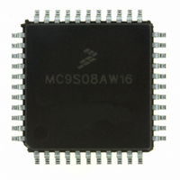
IC MCU 32K FLASH 44-LQFP
Manufacturer
Freescale Semiconductor
Series
HCS08r
Specifications of MC9S08AW32CFGE
Core Processor
HCS08
Core Size
8-Bit
Speed
40MHz
Connectivity
I²C, SCI, SPI
Peripherals
LVD, POR, PWM, WDT
Number Of I /o
34
Program Memory Size
32KB (32K x 8)
Program Memory Type
FLASH
Ram Size
2K x 8
Voltage - Supply (vcc/vdd)
2.7 V ~ 5.5 V
Data Converters
A/D 8x10b
Oscillator Type
Internal
Operating Temperature
-40°C ~ 85°C
Package / Case
44-LQFP
Processor Series
S08AW
Core
HCS08
Data Bus Width
8 bit
Data Ram Size
2 KB
Interface Type
I2C, SCI, SPI
Maximum Clock Frequency
40 MHz
Number Of Programmable I/os
34
Number Of Timers
8
Operating Supply Voltage
- 0.3 V to + 5.8 V
Maximum Operating Temperature
+ 85 C
Mounting Style
SMD/SMT
3rd Party Development Tools
EWS08
Development Tools By Supplier
DEMO9S08AW60E
Minimum Operating Temperature
- 55 C
On-chip Adc
10 bit, 8 Channel
Package
44LQFP
Family Name
HCS08
Maximum Speed
40 MHz
Lead Free Status / RoHS Status
Lead free / RoHS Compliant
Eeprom Size
-
Lead Free Status / Rohs Status
Details
Available stocks
Company
Part Number
Manufacturer
Quantity
Price
Company:

Part Number:
MC9S08AW32CFGE
Manufacturer:
FREESCALE
Quantity:
5 456
Company:
Part Number:
MC9S08AW32CFGE
Manufacturer:
Freescale Semiconductor
Quantity:
10 000
Part Number:
MC9S08AW32CFGE
Manufacturer:
FREESCALE
Quantity:
20 000
Company:
Part Number:
MC9S08AW32CFGER
Manufacturer:
Freescale Semiconductor
Quantity:
10 000


Refer to
as XTAL and EXTAL pins.
Refer to
keyboard inputs.
6.4
Reading and writing of parallel I/O is done through the port data registers. The direction, input or output,
is controlled through the port data direction registers. The parallel I/O port function for an individual pin
is illustrated in the block diagram below.
The data direction control bits determine whether the pin output driver is enabled, and they control what
is read for port data register reads. Each port pin has a data direction register bit. When PTxDDn = 0, the
corresponding pin is an input and reads of PTxD return the pin value. When PTxDDn = 1, the
corresponding pin is an output and reads of PTxD return the last value written to the port data register.
When a peripheral module or system function is in control of a port pin, the data direction register bit still
controls what is returned for reads of the port data register, even though the peripheral system has
overriding control of the actual pin direction.
When a shared analog function is enabled for a pin, all digital pin functions are disabled. A read of the port
data register returns a value of 0 for any bits which have shared analog functions enabled. In general,
whenever a pin is shared with both an alternate digital function and an analog function, the analog function
Freescale Semiconductor
Chapter 8, “Internal Clock Generator
Chapter 9, “Keyboard Interrupt
Parallel I/O Control
Port Read
BUSCLK
Data
PTxDDn
D
D
PTxDn
Figure 6-9. Parallel I/O Block Diagram
MC9S08AC16 Series Data Sheet, Rev. 8
Q
Q
(S08KBIV1)” for more information about using port G pins as
(S08ICGV4)” for more information about using port G pins
1
0
Synchronizer
Output Enable
Output Data
Chapter 6 Parallel Input/Output
Input Data
87
Related parts for MC9S08AW32CFGE
Image
Part Number
Description
Manufacturer
Datasheet
Request
R

Part Number:
Description:
Manufacturer:
Freescale Semiconductor, Inc
Datasheet:
Part Number:
Description:
Manufacturer:
Freescale Semiconductor, Inc
Datasheet:
Part Number:
Description:
Manufacturer:
Freescale Semiconductor, Inc
Datasheet:
Part Number:
Description:
Manufacturer:
Freescale Semiconductor, Inc
Datasheet:
Part Number:
Description:
Manufacturer:
Freescale Semiconductor, Inc
Datasheet:
Part Number:
Description:
Manufacturer:
Freescale Semiconductor, Inc
Datasheet:
Part Number:
Description:
Manufacturer:
Freescale Semiconductor, Inc
Datasheet:
Part Number:
Description:
Manufacturer:
Freescale Semiconductor, Inc
Datasheet:
Part Number:
Description:
Manufacturer:
Freescale Semiconductor, Inc
Datasheet:
Part Number:
Description:
Manufacturer:
Freescale Semiconductor, Inc
Datasheet:
Part Number:
Description:
Manufacturer:
Freescale Semiconductor, Inc
Datasheet:
Part Number:
Description:
Manufacturer:
Freescale Semiconductor, Inc
Datasheet:
Part Number:
Description:
Manufacturer:
Freescale Semiconductor, Inc
Datasheet:
Part Number:
Description:
Manufacturer:
Freescale Semiconductor, Inc
Datasheet:
Part Number:
Description:
Manufacturer:
Freescale Semiconductor, Inc
Datasheet: