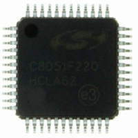
C8051F220-GQ Silicon Laboratories Inc, C8051F220-GQ Datasheet - Page 86

C8051F220-GQ
Manufacturer Part Number
C8051F220-GQ
Description
IC 8051 MCU 8K FLASH 48TQFP
Manufacturer
Silicon Laboratories Inc
Series
C8051F2xxr
Specifications of C8051F220-GQ
Program Memory Type
FLASH
Program Memory Size
8KB (8K x 8)
Package / Case
48-TQFP, 48-VQFP
Core Processor
8051
Core Size
8-Bit
Speed
25MHz
Connectivity
SPI, UART/USART
Peripherals
Brown-out Detect/Reset, POR, WDT
Number Of I /o
32
Ram Size
256 x 8
Voltage - Supply (vcc/vdd)
2.7 V ~ 3.6 V
Data Converters
A/D 32x8b
Oscillator Type
Internal
Operating Temperature
-40°C ~ 85°C
Processor Series
C8051F2x
Core
8051
Data Bus Width
8 bit
Data Ram Size
256 B
Interface Type
SPI/UART
Maximum Clock Frequency
25 MHz
Number Of Programmable I/os
32
Number Of Timers
3
Operating Supply Voltage
2.7 V to 3.6 V
Maximum Operating Temperature
+ 85 C
Mounting Style
SMD/SMT
3rd Party Development Tools
PK51, CA51, A51, ULINK2
Development Tools By Supplier
C8051F206DK
Minimum Operating Temperature
- 40 C
On-chip Adc
32-ch x 8-bit
Lead Free Status / RoHS Status
Lead free / RoHS Compliant
For Use With
336-1241 - DEV KIT F220/221/226/230/231/236
Eeprom Size
-
Lead Free Status / Rohs Status
Lead free / RoHS Compliant
Other names
336-1238
Available stocks
Company
Part Number
Manufacturer
Quantity
Price
Company:
Part Number:
C8051F220-GQ
Manufacturer:
Silicon Laboratories Inc
Quantity:
10 000
Company:
Part Number:
C8051F220-GQR
Manufacturer:
Silicon Laboratories Inc
Quantity:
10 000
C8051F2xx
write/erase operations are disabled. Note that code execution in the 8051 is stalled while the Flash is
being programmed or erased.
Table 10.1. Flash Memory Electrical Characteristics
V
Non-volatile Data Storage
The Flash memory can be used for non-volatile data storage as well as program code. This allows data
such as calibration coefficients to be calculated and stored at run time. Data is written using the MOVX
instruction and read using the MOVC instruction.
The MCU incorporates an additional 128-byte sector of Flash memory located at 0x2000 – 0x207F. This
sector can be used for program code or data storage. However, its smaller sector size makes it particularly
well suited as general purpose, non-volatile scratchpad memory. Even though Flash memory can be writ-
ten a single byte at a time, an entire sector must be erased first. In order to change a single byte of a multi-
byte data set, the data must be moved to temporary storage. Next, the sector is erased, the data set
updated and the data set returned to the original sector. The 128-byte sector-size facilitates updating data
without wasting program memory space by allowing the use of internal data RAM for temporary storage. (A
normal 512-byte sector is too large to be stored in the 256-byte internal data memory.)
10.2. Security Options
The CIP-51 provides security options to protect the Flash memory from inadvertent modification by soft-
ware as well as prevent the viewing of proprietary program code and constants. The Program Store Write
Enable (PSCTL.0) and the Program Store Erase Enable (PSCTL.1) bits protect the Flash memory from
accidental modification by software. These bits must be explicitly set to logic 1 before software can modify
the Flash memory. Additional security features prevent proprietary program code and data constants from
being read or altered across the JTAG interface or by software running on the system controller.
A set of security lock bytes stored at 0x1DFE and 0x1DFF protect the Flash program memory from being
read or altered across the JTAG interface. Each bit in a security lock-byte protects one 1 kB block of mem-
ory. Clearing a bit to logic 0 in a Read lock byte prevents the corresponding block of Flash memory from
being read across the JTAG interface. Clearing a bit in the Write/Erase lock byte protects the block from
JTAG erasures and/or writes. The Read lock byte is at location 0x1DFF. The Write/Erase lock byte is
located at 0x1DFE. Figure 10.1 shows the location and bit definitions of the security bytes. The 512-byte
sector containing the lock byte cannot be erased by software. Writing to the reserved area should not be
performed.
86
Endurance
Erase/Write Cycle Time
DD
= 2.7 to 3.6 V, –40 to +85 ×C unless otherwise specified.
Parameter
Conditions
Rev. 1.6
20 k
Min
—
100 k
Typ
10
Max
—
—
Erase/Wr
Units
ms


