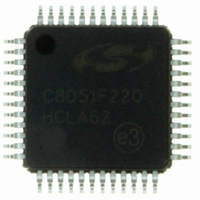
C8051F220-GQ Silicon Laboratories Inc, C8051F220-GQ Datasheet - Page 139

C8051F220-GQ
Manufacturer Part Number
C8051F220-GQ
Description
IC 8051 MCU 8K FLASH 48TQFP
Manufacturer
Silicon Laboratories Inc
Series
C8051F2xxr
Specifications of C8051F220-GQ
Program Memory Type
FLASH
Program Memory Size
8KB (8K x 8)
Package / Case
48-TQFP, 48-VQFP
Core Processor
8051
Core Size
8-Bit
Speed
25MHz
Connectivity
SPI, UART/USART
Peripherals
Brown-out Detect/Reset, POR, WDT
Number Of I /o
32
Ram Size
256 x 8
Voltage - Supply (vcc/vdd)
2.7 V ~ 3.6 V
Data Converters
A/D 32x8b
Oscillator Type
Internal
Operating Temperature
-40°C ~ 85°C
Processor Series
C8051F2x
Core
8051
Data Bus Width
8 bit
Data Ram Size
256 B
Interface Type
SPI/UART
Maximum Clock Frequency
25 MHz
Number Of Programmable I/os
32
Number Of Timers
3
Operating Supply Voltage
2.7 V to 3.6 V
Maximum Operating Temperature
+ 85 C
Mounting Style
SMD/SMT
3rd Party Development Tools
PK51, CA51, A51, ULINK2
Development Tools By Supplier
C8051F206DK
Minimum Operating Temperature
- 40 C
On-chip Adc
32-ch x 8-bit
Lead Free Status / RoHS Status
Lead free / RoHS Compliant
For Use With
336-1241 - DEV KIT F220/221/226/230/231/236
Eeprom Size
-
Lead Free Status / Rohs Status
Lead free / RoHS Compliant
Other names
336-1238
Available stocks
Company
Part Number
Manufacturer
Quantity
Price
Company:
Part Number:
C8051F220-GQ
Manufacturer:
Silicon Laboratories Inc
Quantity:
10 000
Company:
Part Number:
C8051F220-GQR
Manufacturer:
Silicon Laboratories Inc
Quantity:
10 000
18. JTAG
Description
The MCU has an on-chip JTAG interface and logic to support Flash read and write operations and non-
intrusive in-circuit debug. The C8051F2xx may be placed in a JTAG test chain in order to maintain only
one JTAG interface in a system for boundary scan of other parts, and still utilize the C8051F2xx debug and
Flash programming. However, the C8051F2xx does NOT support boundary scan and will act as BYPASS
as specified in IEEE 1149.1.
The JTAG interface is implemented via four dedicated pins on the MCU, which are TCK, TMS, TDI, and
TDO. These pins are all 5 volt tolerant.
Through the 16-bit JTAG Instruction Register (IR), five instructions shown in JTAG Register Definition 18.1
can be commanded. These commands can either select the device ID code, or select registers for Flash
programming operations. BYPASS is shown to illustrate its default setting. There are four Data Registers
associated with the Flash read and write operations on the MCU.
Bit15
IR value
0xFFFF
0x0004
0x0082
0x0083
0x0084
0x0085
Flash Address
Flash Control
Instruction
Flash Scale
Flash Data
BYPASS
IDCODE
JTAG Register Definition 18.1. IR: JTAG Instruction
Selects device ID Register
Selects bypass Data Register and is DEFAULT for the device. Note:
The device does NOT support boundary scan. However, it may be
placed in a scan chain and bypassed in a system of other devices utiliz-
ing boundary scan.
Selects FLASHCON Register to control how the interface logic
responds to reads and writes to the FLASHDAT Register
Selects FLASHDAT Register for reads and writes to the Flash memory
Selects FLASHADR Register which holds the address of all Flash read,
write, and erase operations
Selects FLASHSCL Register which controls the prescaler used to gen-
erate timing signals for Flash operations
Rev. 1.6
Description
C8051F2xx
Bit0
Reset Value
0x0000
139


