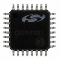
C8051F221-GQR Silicon Laboratories Inc, C8051F221-GQR Datasheet - Page 33

C8051F221-GQR
Manufacturer Part Number
C8051F221-GQR
Description
IC 8051 MCU 8K FLASH 32LQFP
Manufacturer
Silicon Laboratories Inc
Series
C8051F2xxr
Specifications of C8051F221-GQR
Core Processor
8051
Core Size
8-Bit
Speed
25MHz
Connectivity
SPI, UART/USART
Peripherals
Brown-out Detect/Reset, POR, WDT
Number Of I /o
22
Program Memory Size
8KB (8K x 8)
Program Memory Type
FLASH
Ram Size
256 x 8
Voltage - Supply (vcc/vdd)
2.7 V ~ 3.6 V
Data Converters
A/D 22x8b
Oscillator Type
Internal
Operating Temperature
-40°C ~ 85°C
Package / Case
32-LQFP
Processor Series
C8051F2x
Core
8051
Data Bus Width
8 bit
Data Ram Size
256 B
Interface Type
SPI, UART
Maximum Clock Frequency
25 MHz
Number Of Programmable I/os
32
Number Of Timers
3 bit
Operating Supply Voltage
2.7 V to 3.6 V
Maximum Operating Temperature
+ 85 C
Mounting Style
SMD/SMT
3rd Party Development Tools
PK51, CA51, A51, ULINK2
Development Tools By Supplier
C8051F226DK
Minimum Operating Temperature
- 40 C
On-chip Adc
8 bit, 32 Channel
For Use With
336-1241 - DEV KIT F220/221/226/230/231/236
Lead Free Status / RoHS Status
Lead free / RoHS Compliant
Eeprom Size
-
Lead Free Status / Rohs Status
Details
Available stocks
Company
Part Number
Manufacturer
Quantity
Price
Company:
Part Number:
C8051F221-GQR
Manufacturer:
Silicon Laboratories Inc
Quantity:
10 000
5.2.
The ADC has a maximum conversion speed of 100ksps. The ADC conversion clock is derived from the
system clock. The ADC conversion clock is derived from a divided version of SYSCLK. Divide ratios of
1,2,4,8, or 16 are supported by setting the ADCSC bits in the ADC0CF Register. This is useful to adjust
conversion speed to accommodate different system clock speeds.
A conversion can be initiated in one of two ways, depending on the programmed states of the ADC Start of
Conversion Mode bits (ADSTM1, ADSTM0) in ADC0CN. Conversions may be initiated by:
Writing a 1 to ADBUSY provides software control of the ADC whereby conversions are performed "on-
demand". During conversion, the ADBUSY bit is set to 1 and restored to 0 when conversion is complete.
The falling edge of ADBUSY triggers an interrupt (when enabled) and sets the ADCINT interrupt flag in the
ADC0CN register. Note: When conversions are performed "on-demand", the ADCINT flag, not ADBUSY,
should be polled to determine when the conversion has completed. Converted data is available in the ADC
data word register, ADC0H.
The ADCTM bit in register ADC0CN controls the ADC track-and-hold mode. In its default state, the ADC
input is continuously tracked, except when a conversion is in progress. Setting ADCTM to 1 allows one of
two different low power track-and-hold modes to be specified by states of the ADSTM1-0 bits (also in
ADC0CN):
Tracking can be disabled (shutdown) when the entire chip is in low power standby or sleep modes.
ADC Modes of Operation
1. Writing a 1 to the ADBUSY bit of ADC0CN;
2. A Timer 2 overflow (i.e., timed continuous conversions).
1. Tracking begins with a write of 1 to ADBUSY and lasts for 3 SAR clocks;
2. Tracking starts with an overflow of Timer 2 and lasts for 3 SAR clocks.
Timer2, Timer3 Overflow;
(ADSTM[1:0]=00, 01, 11)
Write 1 to ADBUSY
Figure 5.2. 12-Bit ADC Track and Conversion Example Timing
(ADSTM[1:0]=10)
SAR Clocks
SAR Clocks
SAR Clocks
ADCTM=1
ADCTM=0
ADCTM=1
ADCTM=0
CNVSTR
A. ADC Timing for External Trigger Source
B. ADC Timing for Internal Trigger Sources
Track or Convert
Low Power or
Low Power or
Convert
Convert
Track Or Convert
1
1
Track
2
2
Track
3
3
4
4
1
5
5
2
6
6
Rev. 1.6
3
7
7
Convert
4
8
8
5
9
9
10 11 12 13 14 15 16 17 18 19
10 11 12 13 14 15 16
6
Convert
7
Convert
Convert
8
9
10 11 12 13 14 15 16
Low Power Mode
Track
Low Power Mode
C8051F2xx
Track
33


