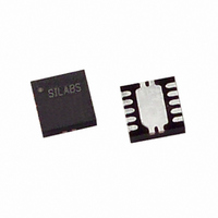
C8051F305-GMR Silicon Laboratories Inc, C8051F305-GMR Datasheet - Page 90

C8051F305-GMR
Manufacturer Part Number
C8051F305-GMR
Description
IC 8051 MCU 2K FLASH 11QFN
Manufacturer
Silicon Laboratories Inc
Series
C8051F30xr
Specifications of C8051F305-GMR
Core Processor
8051
Core Size
8-Bit
Speed
25MHz
Connectivity
SMBus (2-Wire/I²C), UART/USART
Peripherals
POR, PWM, WDT
Number Of I /o
8
Program Memory Size
2KB (2K x 8)
Program Memory Type
FLASH
Ram Size
256 x 8
Voltage - Supply (vcc/vdd)
2.7 V ~ 3.6 V
Oscillator Type
External
Operating Temperature
-40°C ~ 85°C
Package / Case
11-VQFN
For Use With
336-1444 - ADAPTER PROGRAM TOOLSTICK F300
Lead Free Status / RoHS Status
Lead free / RoHS Compliant
Eeprom Size
-
Data Converters
-
Available stocks
Company
Part Number
Manufacturer
Quantity
Price
Part Number:
C8051F305-GMR
Manufacturer:
SILICONLABS/芯科
Quantity:
20 000
C8051F300/1/2/3/4/5
10.1.3. Flash Write Procedure
Flash bytes are programmed by software with the following sequence:
Steps 5–7 must be repeated for each byte to be written. After Flash writes are complete, PSWE should be
cleared so that MOVX instructions do not target program memory. Writing to and erasing the Reserved
area of Flash should be avoided.
10.2. Non-Volatile Data Storage
The Flash memory can be used for non-volatile data storage as well as program code. This allows data
such as calibration coefficients to be calculated and stored at run time. Data is written using the MOVX
instruction and read using the MOVC instruction.
10.3. Security Options
The CIP-51 provides security options to protect the Flash memory from inadvertent modification by soft-
ware as well as to prevent the viewing of proprietary program code and constants. The Program Store
Write Enable (bit PSWE in register PSCTL) and the Program Store Erase Enable (bit PSEE in register
PSCTL) bits protect the Flash memory from accidental modification by software. PSWE must be explicitly
set to ‘1’ before software can modify the Flash memory; both PSWE and PSEE must be set to ‘1’ before
software can erase Flash memory. Additional security features prevent proprietary program code and data
constants from being read or altered across the C2 interface.
A security lock byte stored at the last byte of Flash user space protects the Flash program memory from
being read or altered across the C2 interface. See Table 10.2 for the security byte description; see
Figure 10.1 for a program memory map and the security byte locations for each device.
90
*Note: 512 bytes at location 0x1E00 to 0x1FFF are reserved.
writes from application code)
SYSCLK Frequency (Flash
Erase Cycle Time
Write Cycle Time
Step 1. Disable interrupts (recommended).
Step 2. Erase the 512-byte Flash page containing the target location, as described in
Step 3. Set the PSWE bit in PSCTL.
Step 4. Clear the PSEE bit in PSCTL.
Step 5. Write the first key code to FLKEY: 0xA5.
Step 6. Write the second key code to FLKEY: 0xF1.
Step 7. Using the MOVX instruction, write a single data byte to the desired location within the 512-
Parameter
Endurance
Flash Size
10.1.2.
byte sector.
Table 10.1. Flash Electrical Characteristics
25 MHz System Clock
25 MHz System Clock
C8051F300/1/2/3
Conditions
C8051F304
C8051F305
Rev. 2.9
8192*
4096
2048
Min
20k
100
10
40
100k
Typ
15
55
Max
20
70
Erase/Write
Section
Units
bytes
bytes
bytes
kHz
ms
µs


