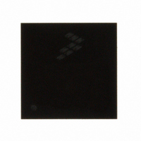
MC9S08GT8ACFDE Freescale Semiconductor, MC9S08GT8ACFDE Datasheet - Page 212

MC9S08GT8ACFDE
Manufacturer Part Number
MC9S08GT8ACFDE
Description
IC MCU 8K FLASH 1K RAM 48-QFN
Manufacturer
Freescale Semiconductor
Series
HCS08r
Datasheet
1.MC9S08GT8ACFBER.pdf
(300 pages)
Specifications of MC9S08GT8ACFDE
Core Processor
HCS08
Core Size
8-Bit
Speed
40MHz
Connectivity
I²C, SCI, SPI
Peripherals
LVD, POR, PWM, WDT
Number Of I /o
39
Program Memory Size
8KB (8K x 8)
Program Memory Type
FLASH
Ram Size
1K x 8
Voltage - Supply (vcc/vdd)
1.8 V ~ 3.6 V
Data Converters
A/D 8x10b
Oscillator Type
Internal
Operating Temperature
-40°C ~ 85°C
Package / Case
48-QFN
Processor Series
S08GT
Core
HCS08
Data Bus Width
8 bit
Data Ram Size
1 KB
Interface Type
I2C/SCI/SPI
Maximum Clock Frequency
40 MHz
Number Of Programmable I/os
39
Operating Supply Voltage
3.6 V
Maximum Operating Temperature
+ 85 C
Mounting Style
SMD/SMT
3rd Party Development Tools
EWS08
Development Tools By Supplier
M68EVB908GB60E, M68DEMO908GB60E
Minimum Operating Temperature
- 40 C
On-chip Adc
8-ch x 10-bit
For Use With
M68DEMO908GB60E - BOARD DEMO MC9S08GB60M68EVB908GB60E - BOARD EVAL FOR MC9S08GB60
Lead Free Status / RoHS Status
Lead free / RoHS Compliant
Eeprom Size
-
Lead Free Status / Rohs Status
Lead free / RoHS Compliant
- Current page: 212 of 300
- Download datasheet (2Mb)
Inter-Integrated Circuit (S08IICV1)
13.3.3
212
Reset
IICEN
TXAK
RSTA
Field
IICIE
MST
TX
7
6
5
4
3
2
W
R
IICEN
IIC Control Register (IICC)
IIC Enable — The IICEN bit determines whether the IIC module is enabled.
0 IIC is not enabled.
1 IIC is enabled.
IIC Interrupt Enable — The IICIE bit determines whether an IIC interrupt is requested.
0 IIC interrupt request not enabled.
1 IIC interrupt request enabled.
Master Mode Select — The MST bit is changed from a 0 to a 1 when a START signal is generated on the bus
and master mode is selected. When this bit changes from a 1 to a 0 a STOP signal is generated and the mode
of operation changes from master to slave.
0 Slave Mode.
1 Master Mode.
Transmit Mode Select — The TX bit selects the direction of master and slave transfers. In master mode this bit
should be set according to the type of transfer required. Therefore, for address cycles, this bit will always be high.
When addressed as a slave this bit should be set by software according to the SRW bit in the status register.
0 Receive.
1 Transmit.
Transmit Acknowledge Enable — This bit specifies the value driven onto the SDA during data acknowledge
cycles for both master and slave receivers.
0 An acknowledge signal will be sent out to the bus after receiving one data byte.
1 No acknowledge signal response is sent.
Repeat START — Writing a one to this bit will generate a repeated START condition provided it is the current
master. This bit will always be read as a low. Attempting a repeat at the wrong time will result in loss of arbitration.
0
7
= Unimplemented or Reserved
IICIE
0
6
Table 13-4. IICC Register Field Descriptions
Figure 13-5. IIC Control Register (IICC)
MC9S08GT16A/GT8A Data Sheet, Rev. 1
MST
0
5
TX
0
4
Description
TXAK
3
0
RSTA
0
0
2
Freescale Semiconductor
0
0
1
0
0
0
Related parts for MC9S08GT8ACFDE
Image
Part Number
Description
Manufacturer
Datasheet
Request
R
Part Number:
Description:
Manufacturer:
Freescale Semiconductor, Inc
Datasheet:
Part Number:
Description:
Manufacturer:
Freescale Semiconductor, Inc
Datasheet:
Part Number:
Description:
Manufacturer:
Freescale Semiconductor, Inc
Datasheet:
Part Number:
Description:
Manufacturer:
Freescale Semiconductor, Inc
Datasheet:
Part Number:
Description:
Manufacturer:
Freescale Semiconductor, Inc
Datasheet:
Part Number:
Description:
Manufacturer:
Freescale Semiconductor, Inc
Datasheet:
Part Number:
Description:
Manufacturer:
Freescale Semiconductor, Inc
Datasheet:
Part Number:
Description:
Manufacturer:
Freescale Semiconductor, Inc
Datasheet:
Part Number:
Description:
Manufacturer:
Freescale Semiconductor, Inc
Datasheet:
Part Number:
Description:
Manufacturer:
Freescale Semiconductor, Inc
Datasheet:
Part Number:
Description:
Manufacturer:
Freescale Semiconductor, Inc
Datasheet:
Part Number:
Description:
Manufacturer:
Freescale Semiconductor, Inc
Datasheet:
Part Number:
Description:
Manufacturer:
Freescale Semiconductor, Inc
Datasheet:
Part Number:
Description:
Manufacturer:
Freescale Semiconductor, Inc
Datasheet:
Part Number:
Description:
Manufacturer:
Freescale Semiconductor, Inc
Datasheet:


