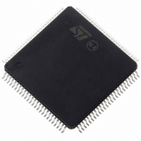
ST10F269Z2T3 STMicroelectronics, ST10F269Z2T3 Datasheet - Page 137

ST10F269Z2T3
Manufacturer Part Number
ST10F269Z2T3
Description
MCU 16BIT 256KBIT FLASH 144-TQFP
Manufacturer
STMicroelectronics
Series
ST10r
Datasheet
1.ST10F269Z2Q3.pdf
(184 pages)
Specifications of ST10F269Z2T3
Core Processor
ST10
Core Size
16-Bit
Speed
40MHz
Connectivity
CAN, EBI/EMI, SSC, UART/USART
Peripherals
POR, PWM, WDT
Number Of I /o
111
Program Memory Size
256KB (256K x 8)
Program Memory Type
FLASH
Ram Size
12K x 8
Voltage - Supply (vcc/vdd)
4.5 V ~ 5.5 V
Data Converters
A/D 16x10b
Oscillator Type
Internal
Operating Temperature
-40°C ~ 125°C
Package / Case
144-TQFP, 144-VQFP
Processor Series
ST10F26x
Core
ST10
Data Bus Width
16 bit
Data Ram Size
12 KB
Interface Type
CAN, SSC, USART
Maximum Clock Frequency
40 MHz
Number Of Programmable I/os
111
Number Of Timers
5
Maximum Operating Temperature
+ 125 C
Mounting Style
SMD/SMT
Minimum Operating Temperature
- 40 C
On-chip Adc
10 bit, 16 Channel
Lead Free Status / RoHS Status
Lead free / RoHS Compliant
Eeprom Size
-
Lead Free Status / Rohs Status
Details
Available stocks
Company
Part Number
Manufacturer
Quantity
Price
Company:
Part Number:
ST10F269Z2T3
Manufacturer:
LITTLEFUSE
Quantity:
1 000
Company:
Part Number:
ST10F269Z2T3
Manufacturer:
STMicroelectronics
Quantity:
10 000
ST10F269
xxIC (yyyyh / zzh)
XPERCON (F024h / 12h)
CAN1EN
CAN2EN
XRAM1EN
XRAM2EN
RTCEN
15
15
-
-
GLVL
ILVL
14
xxIE
xxIR
Bit
-
14
-
13
-
CAN1 Enable Bit
‘0’: Accesses to the on-chip CAN1 XPeripheral and its functions are disabled. P4.5 and P4.6 pins can be
used as general purpose I/Os. Address range 00’EF00h-00’EFFFh is only directed to external memory if
CAN2EN is also ‘0’.
‘1’: The on-chip CAN1 XPeripheral is enabled and can be accessed.
CAN2 Enable Bit
‘0’: Accesses to the on-chip CAN2 XPeripheral and its functions are disabled. P4.4 and P4.7 pins can be
used as general purpose I/Os. Address range 00’EE00h-00’EEFFh is only directed to external memory if
CAN1EN is also ‘0’.
‘1’: The on-chip CAN2 XPeripheral is enabled and can be accessed.
XRAM1 Enable Bit
‘0’: Accesses to external memory within space 00’E000h to 00’E7FFh. The 2K Bytes of internal XRAM1
are disabled.
’1’: Accesses to the internal 2K Bytes of XRAM1.
XRAM2 Enable Bit
‘0’: Accesses to the external memory within space 00’C000h to 00’DFFFh. The 8K Bytes of internal
XRAM2 are disabled.
’1’: Accesses to the internal 8K Bytes of XRAM2.
RTC Enable Bit
’0’: Accesses to the on-chip Real Time Clock are disabled, external access performed. Address range
00’EC00h-00’ECFFh is only directed to external memory if CAN1EN and CAN2EN are ’0’ also
13
-
12
-
Group Level
Defines the internal order for simultaneous requests of the same priority.
3: Highest group priority
0: Lowest group priority
Interrupt Priority Level
Defines the priority level for the arbitration of requests.
Fh: Highest priority level
0h: Lowest priority level
Interrupt Enable Control Bit (individually enables/disables a specific source)
‘0’: Interrupt Request is disabled
‘1’: Interrupt Request is enabled
Interrupt Request Flag
‘0’: No request pending
‘1’: This source has raised an interrupt request
11
12
-
-
10
-
11
-
9
-
10
-
8
-
9
-
7
-
20 - SPECIAL FUNCTION REGISTER OVERVIEW
SFR Area
6
-
8
-
ESFR
5
-
xxIR
RW
7
RTCEN
Function
RW
4
xxIE
RW
6
XRAM2EN
RW
3
5
XRAM1EN
4
ILVL
RW
RW
2
3
Reset Value: --00h
Reset Value: --05h
CAN2EN
RW
2
1
1
GLVL
CAN1EN
RW
137/184
RW
0
0


