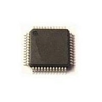
STM32F102CBT6TR STMicroelectronics, STM32F102CBT6TR Datasheet - Page 58

STM32F102CBT6TR
Manufacturer Part Number
STM32F102CBT6TR
Description
MCU 32BIT ARM 128K FLASH 48-LQFP
Manufacturer
STMicroelectronics
Series
STM32r
Datasheet
1.STEVAL-MKI109V1.pdf
(69 pages)
Specifications of STM32F102CBT6TR
Core Processor
ARM® Cortex-M3™
Core Size
32-Bit
Speed
48MHz
Connectivity
I²C, IrDA, LIN, SPI, UART/USART, USB
Peripherals
DMA, PDR, POR, PVD, PWM, Temp Sensor, WDT
Number Of I /o
37
Program Memory Size
128KB (128K x 8)
Program Memory Type
FLASH
Ram Size
16K x 8
Voltage - Supply (vcc/vdd)
2 V ~ 3.6 V
Data Converters
A/D 10x12b
Oscillator Type
Internal
Operating Temperature
-40°C ~ 85°C
Package / Case
48-LQFP
Processor Series
STM32F102x
Core
ARM Cortex M3
Data Bus Width
32 bit
Data Ram Size
16 KB
Interface Type
I2C, SPI, USART
Maximum Clock Frequency
48 MHz
Number Of Programmable I/os
37
Number Of Timers
6
Operating Supply Voltage
2 V to 3.6 V
Maximum Operating Temperature
+ 85 C
Mounting Style
SMD/SMT
3rd Party Development Tools
EWARM, EWARM-BL, MDK-ARM, RL-ARM, ULINK2
Minimum Operating Temperature
- 40 C
On-chip Adc
12 bit, 10 Channel
For Use With
497-10030 - STARTER KIT FOR STM32497-6438 - BOARD EVALUTION FOR STM32 512K
Lead Free Status / RoHS Status
Lead free / RoHS Compliant
Eeprom Size
-
Lead Free Status / Rohs Status
Details
Available stocks
Company
Part Number
Manufacturer
Quantity
Price
Company:
Part Number:
STM32F102CBT6TR
Manufacturer:
STMicroelectronics
Quantity:
10 000
Electrical characteristics
58/69
Table 44.
1. Guaranteed by design, not tested in production.
2. V
3. For external triggers, a delay of 1/f
Equation 1: R
The formula above
error below 1/4 of LSB. Here N = 12 (from 12-bit resolution).
t
Symbol
STAB
t
R
C
f
R
CONV
t
TRIG
t
V
CAL
t
f
V
ADC
ADC
R
f
latr
t
AIN
lat
ADC
S
S
DDA
AIN
REF+
AIN
(1)
(1)
(1)
(1)
(1)
(1)
(1)
(1)
(1)
(1)
(1)
is internally connected to V
------------------------------------------------------------- - R
f
ADC
Power supply
ADC clock frequency
Sampling rate
External trigger frequency
Conversion voltage range
External input impedance
Sampling switch resistance
Internal sample and hold
capacitor
Calibration time
Injection trigger conversion
latency
Regular trigger conversion
latency
Sampling time
Power-up time
Total conversion time
(including sampling time)
ADC characteristics
AIN
C
(Equation
ADC
Parameter
max formula:
T
S
ln
1) is used to determine the maximum external impedance allowed for an
2
N
+
DDA
Doc ID 15056 Rev 3
PCLK2
2
(2)
–
and V
must be added to the latency specified in
ADC
See
f
f
f
f
f
f
ADC
ADC
ADC
ADC
ADC
ADC
and
REF-
Conditions
for details
Equation 1
= 12 MHz
= 12 MHz
= 12 MHz
= 12 MHz
= 12 MHz
= 12 MHz
Table 45
is internally connected to V
14 to 252 (t
for successive approximation)
V
0 (V
REF-
ground)
0.107
0.05
Min
2.4
0.6
1.5
1.2
SSA
0
tied to
STM32F102x8, STM32F102xB
or
S
for sampling +12.5
SSA
5.9
83
Typ
,
0
Table
44.
V
0.214
0.143
239.5
Max
17.1
823
3
2
3.6
REF+
12
17
50
18
1
1
1
8
(3)
(3)
1/f
1/f
1/f
1/f
1/f
1/f
MHz
MHz
Unit
kHz
k
k
pF
µs
µs
µs
µs
µs
µs
V
V
ADC
ADC
ADC
ADC
ADC
ADC


