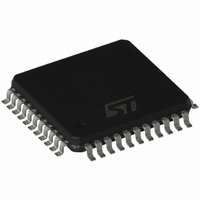
ST72F361J9T6 STMicroelectronics, ST72F361J9T6 Datasheet - Page 193

ST72F361J9T6
Manufacturer Part Number
ST72F361J9T6
Description
IC MCU 8BIT 60K FLASH 44-LQFP
Manufacturer
STMicroelectronics
Series
ST7r
Datasheet
1.ST72F361K6T6.pdf
(225 pages)
Specifications of ST72F361J9T6
Core Processor
ST7
Core Size
8-Bit
Speed
8MHz
Connectivity
LINSCI, SPI
Peripherals
LVD, POR, PWM, WDT
Number Of I /o
32
Program Memory Size
60KB (60K x 8)
Program Memory Type
FLASH
Ram Size
2K x 8
Voltage - Supply (vcc/vdd)
3.8 V ~ 5.5 V
Data Converters
A/D 16x10b
Oscillator Type
External
Operating Temperature
-40°C ~ 85°C
Package / Case
44-LQFP
Processor Series
ST72F3x
Core
ST7
Data Bus Width
8 bit
Data Ram Size
2 KB
Interface Type
LINSCI, SPI
Maximum Clock Frequency
8 MHz
Number Of Programmable I/os
34
Number Of Timers
2
Maximum Operating Temperature
+ 85 C
Mounting Style
SMD/SMT
Development Tools By Supplier
ST72F36X-SK/RAIS, STX-RLINK
Minimum Operating Temperature
- 40 C
On-chip Adc
10 bit, 11 Channel
Lead Free Status / RoHS Status
Lead free / RoHS Compliant
Eeprom Size
-
Lead Free Status / Rohs Status
Details
Available stocks
Company
Part Number
Manufacturer
Quantity
Price
Company:
Part Number:
ST72F361J9T6
Manufacturer:
STMicroelectronics
Quantity:
50
Company:
Part Number:
ST72F361J9T6
Manufacturer:
STMicroelectronics
Quantity:
10 000
- Current page: 193 of 225
- Download datasheet (8Mb)
12.9 I/O PORT PIN CHARACTERISTICS
12.9.1 General Characteristics
Subject to general operating conditions for V
Notes:
1. Data based on characterization results, not tested in production.
2. Hysteresis voltage between Schmitt trigger switching levels. Based on characterization results, not tested.
3. When the current limitation is not possible, the V
I
to
4. Leakage could be higher than max. if negative current is injected on adjacent pins.
5. Configuration not recommended, all unused pins must be kept at a fixed voltage: Using the output mode of the I/O, for
example, or an external pull-up or pull-down resistor (see
ogy characteristics, not tested in production.
6. The R
scribed in
7. To generate an external interrupt, a minimum pulse width must be applied on an I/O port pin configured as an external
interrupt source.
ΣI
INJ(PIN)
Symbol
I
t
t
INJ(PIN)
INJ(PIN)
t
Section 12.2 on page 179
r(IO)out
f(IO)out
w(IT)in
V
V
R
C
V
V
V
V
I
I
lkg
hys
hys
PU
S
IH
IH
IO
IL
IL
specification. A positive injection is induced by V
PU
3)
Figure
pull-up equivalent resistor is based on a resistive transistor (corresponding I
Input low level voltage
Input high level voltage
Schmitt trigger voltage hysteresis
Input low level voltage
Input high level voltage
Schmitt trigger voltage hysteresis
Injected Current on PB3
Injected Current on any other I/O pin
Total injected current (sum of all I/O
and control pins)
Input leakage current on robust pins See
Input leakage current
Static current consumption
Weak pull-up equivalent resistor
I/O pin capacitance
Output high to low level fall time
Output low to high level rise time
External interrupt pulse time
104).
Parameter
for more details.
7)
4)
1)
1)
1)
1)
5)
7)
6)
2)
2)
CMOS ports
TTL ports
V
V
Floating input mode
V
C
Between 10% and 90%
DD
IN
DD
SS
IN
L
= 50pF
absolute maximum rating must be respected, otherwise refer to
=
, f
≤
“10-BIT ADC CHARACTERISTICS” on page 204
= 5V
IN
V
OSC
V
Conditions
SS
> V
IN
Figure
≤
, and T
Flash devices
ROM devices
V
DD
V
DD
DD
while a negative injection is induced by V
103). Data based on design simulation and/or technol-
= 5V
A
unless otherwise specified.
0.7 x V
Min
50
2
0
1
DD
PU
Typ
400
200
current characteristics de-
90
25
1
5
0.3 x V
Max
±25
250
0.8
+4
±4
±4
±1
IN
DD
< V
ST72361
SS
193/225
Unit
t
. Refer
mV
mA
CPU
μA
kΩ
pF
ns
V
Related parts for ST72F361J9T6
Image
Part Number
Description
Manufacturer
Datasheet
Request
R

Part Number:
Description:
STMicroelectronics [RIPPLE-CARRY BINARY COUNTER/DIVIDERS]
Manufacturer:
STMicroelectronics
Datasheet:

Part Number:
Description:
STMicroelectronics [LIQUID-CRYSTAL DISPLAY DRIVERS]
Manufacturer:
STMicroelectronics
Datasheet:

Part Number:
Description:
BOARD EVAL FOR MEMS SENSORS
Manufacturer:
STMicroelectronics
Datasheet:

Part Number:
Description:
NPN TRANSISTOR POWER MODULE
Manufacturer:
STMicroelectronics
Datasheet:

Part Number:
Description:
TURBOSWITCH ULTRA-FAST HIGH VOLTAGE DIODE
Manufacturer:
STMicroelectronics
Datasheet:

Part Number:
Description:
Manufacturer:
STMicroelectronics
Datasheet:

Part Number:
Description:
DIODE / SCR MODULE
Manufacturer:
STMicroelectronics
Datasheet:

Part Number:
Description:
DIODE / SCR MODULE
Manufacturer:
STMicroelectronics
Datasheet:

Part Number:
Description:
Search -----> STE16N100
Manufacturer:
STMicroelectronics
Datasheet:

Part Number:
Description:
Search ---> STE53NA50
Manufacturer:
STMicroelectronics
Datasheet:

Part Number:
Description:
NPN Transistor Power Module
Manufacturer:
STMicroelectronics
Datasheet:

Part Number:
Description:
DIODE / SCR MODULE
Manufacturer:
STMicroelectronics
Datasheet:


