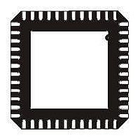
STM32F103C6U6A STMicroelectronics, STM32F103C6U6A Datasheet - Page 72

STM32F103C6U6A
Manufacturer Part Number
STM32F103C6U6A
Description
MCU 32BIT ARM 32K FLASH 48-QFN
Manufacturer
STMicroelectronics
Series
STM32r
Datasheet
1.STM32F103C4T6A.pdf
(87 pages)
Specifications of STM32F103C6U6A
Core Processor
ARM® Cortex-M3™
Core Size
32-Bit
Speed
72MHz
Connectivity
CAN, I²C, IrDA, LIN, SPI, UART/USART, USB
Peripherals
DMA, Motor Control PWM, PDR, POR, PVD, PWM, Temp Sensor, WDT
Number Of I /o
37
Program Memory Size
32KB (32K x 8)
Program Memory Type
FLASH
Ram Size
10K x 8
Voltage - Supply (vcc/vdd)
2 V ~ 3.6 V
Data Converters
A/D 10x12b
Oscillator Type
Internal
Operating Temperature
-40°C ~ 85°C
Package / Case
48-LQFP
Processor Series
STM32F103x
Core
ARM Cortex M3
Data Bus Width
32 bit
Data Ram Size
10 KB
Interface Type
CAN, I2C, SPI, USART
Maximum Clock Frequency
72 MHz
Number Of Programmable I/os
37
Number Of Timers
6
Operating Supply Voltage
2 V to 3.6 V
Maximum Operating Temperature
+ 85 C
Mounting Style
SMD/SMT
3rd Party Development Tools
EWARM, EWARM-BL, MDK-ARM, RL-ARM, ULINK2
Minimum Operating Temperature
- 40 C
On-chip Adc
12 bit, 10 Channel
For Use With
497-10030 - STARTER KIT FOR STM32497-8511 - KIT STARTER FOR STM32 512K FLASH497-6438 - BOARD EVALUTION FOR STM32 512K
Lead Free Status / RoHS Status
Lead free / RoHS Compliant
Eeprom Size
-
Lead Free Status / Rohs Status
Details
Available stocks
Company
Part Number
Manufacturer
Quantity
Price
Electrical characteristics
72/87
Figure 35. Typical connection diagram using the ADC
1. Refer to
2. C
General PCB design guidelines
Power supply decoupling should be performed as shown
depending on whether V
ceramic (good quality). They should be placed them as close as possible to the chip.
Figure 36. Power supply and reference decoupling (V
1. The V
pad capacitance (roughly 7 pF). A high C
this, f
parasitic
ADC
V AIN
REF+
Table 46
represents the capacitance of the PCB (dependent on soldering and PCB layout quality) plus the
should be reduced.
R AIN (1)
input is available only on the TFBGA64 package.
for the values of R
C parasitic
AINx
REF+
is connected to V
Doc ID 15060 Rev 5
AIN
V DD
, R
parasitic
ADC
0.6 V
0.6 V
V T
V T
and C
value will downgrade conversion accuracy. To remedy
ADC
I L ±1 µA
DDA
.
or not. The 10 nF capacitors should be
R ADC (1)
Sample and hold ADC
converter
inFigure 36
REF+
STM32F103x4, STM32F103x6
C ADC (1)
STM32F103xx
converter
not connected to
12-bit
or
Figure
37,
ai14150c
V
DDA
)


