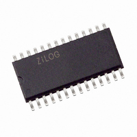
Z8F0412SJ020SG Zilog, Z8F0412SJ020SG Datasheet - Page 145

Z8F0412SJ020SG
Manufacturer Part Number
Z8F0412SJ020SG
Description
IC ENCORE MCU FLASH 4K 28SOIC
Manufacturer
Zilog
Series
Encore!® XP®r
Datasheet
1.Z8F08200100KIT.pdf
(264 pages)
Specifications of Z8F0412SJ020SG
Core Processor
Z8
Core Size
8-Bit
Speed
20MHz
Connectivity
I²C, IrDA, SPI, UART/USART
Peripherals
Brown-out Detect/Reset, POR, PWM, WDT
Number Of I /o
19
Program Memory Size
4KB (4K x 8)
Program Memory Type
FLASH
Ram Size
1K x 8
Voltage - Supply (vcc/vdd)
2.7 V ~ 3.6 V
Oscillator Type
Internal
Operating Temperature
0°C ~ 70°C
Package / Case
28-SOIC (7.5mm Width)
Processor Series
Z8F041xx
Core
eZ8
Data Bus Width
8 bit
Data Ram Size
1 KB
Interface Type
I2C, SPI, UART
Maximum Clock Frequency
20 MHz
Number Of Programmable I/os
19
Number Of Timers
2
Operating Supply Voltage
2.7 V to 3.6 V
Maximum Operating Temperature
+ 70 C
Mounting Style
SMD/SMT
Minimum Operating Temperature
0 C
Lead Free Status / RoHS Status
Lead free / RoHS Compliant
Eeprom Size
-
Data Converters
-
Lead Free Status / Rohs Status
Details
Other names
269-4107
Z8F0412SJ020SG
Z8F0412SJ020SG
Available stocks
Company
Part Number
Manufacturer
Quantity
Price
Part Number:
Z8F0412SJ020SG
Manufacturer:
ZILOG
Quantity:
20 000
- Current page: 145 of 264
- Download datasheet (6Mb)
PS022517-0508
Write Transaction with a 7-Bit Address
Figure 27
indicate data transferred from the I
data transferred from the slaves to the I
Follow the steps below for a transmit operation to a 7-bit addressed slave:
1. Software asserts the IEN bit in the I
2. Software asserts the TXI bit of the I
3. The I
4. Software responds to the TDRE bit by writing a 7-bit Slave address plus write bit (=0)
5. Software asserts the START bit of the I
6. The I
7. The I
8. After one bit of address has been shifted out by the SDA signal, the Transmit Interrupt
9. Software responds by writing the transmit data into the I
10. The I
11. If the I
12. The I
13. The I
S
to the I
Register.
is asserted (TDRE = 1).
next high period of SCL the I
Continue with
If the slave does not acknowledge, the Not Acknowledge interrupt occurs (NCKI bit is
set in the Status register, ACK bit is cleared). Software responds to the Not
Acknowledge interrupt by setting the STOP and FLUSH bits and clearing the TXI bit.
The I
NCKI bits. The transaction is complete (ignore following steps).
I
sent, the Transmit Interrupt is asserted.
2
C Data Register.
Slave Address
2
2
2
2
2
2
2
displays the data transfer format for a 7-bit addressed slave. Shaded regions
C interrupt asserts, because the I
C Controller sends the START condition to the I
C Controller loads the I
C Controller shifts the rest of the address and write bit out by the SDA signal.
C Controller sends the STOP condition on the bus and clears the STOP and
C Controller loads the contents of the I
C Controller shifts the data out of using the SDA signal. After the first bit is
2
2
C Slave sends an acknowledge (by pulling the SDA signal low) during the
C Data Register.
Figure 27. 7-Bit Addressed Slave Data Transfer Format
step
12.
W = 0
A
2
2
C Controller sets the ACK bit in the I
2
C Shift register with the contents of the I
C Controller to slaves and unshaded regions indicate
2
2
C Controller.
Data
2
C Control Register.
C Control Register to enable Transmit Interrupts.
2
2
C Data Register is empty.
C Control Register.
2
A
C Shift register with the contents of the
Z8 Encore! XP
Data
2
C Slave.
2
C Data Register.
Product Specification
A
Data
2
C Status register.
®
F0822 Series
2
C Data
I2C Controller
A/A P/S
132
Related parts for Z8F0412SJ020SG
Image
Part Number
Description
Manufacturer
Datasheet
Request
R

Part Number:
Description:
Communication Controllers, ZILOG INTELLIGENT PERIPHERAL CONTROLLER (ZIP)
Manufacturer:
Zilog, Inc.
Datasheet:

Part Number:
Description:
KIT DEV FOR Z8 ENCORE 16K TO 64K
Manufacturer:
Zilog
Datasheet:

Part Number:
Description:
KIT DEV Z8 ENCORE XP 28-PIN
Manufacturer:
Zilog
Datasheet:

Part Number:
Description:
DEV KIT FOR Z8 ENCORE 8K/4K
Manufacturer:
Zilog
Datasheet:

Part Number:
Description:
KIT DEV Z8 ENCORE XP 28-PIN
Manufacturer:
Zilog
Datasheet:

Part Number:
Description:
DEV KIT FOR Z8 ENCORE 4K TO 8K
Manufacturer:
Zilog
Datasheet:

Part Number:
Description:
CMOS Z8 microcontroller. ROM 16 Kbytes, RAM 256 bytes, speed 16 MHz, 32 lines I/O, 3.0V to 5.5V
Manufacturer:
Zilog, Inc.
Datasheet:

Part Number:
Description:
Low-cost microcontroller. 512 bytes ROM, 61 bytes RAM, 8 MHz
Manufacturer:
Zilog, Inc.
Datasheet:

Part Number:
Description:
Z8 4K OTP Microcontroller
Manufacturer:
Zilog, Inc.
Datasheet:

Part Number:
Description:
CMOS SUPER8 ROMLESS MCU
Manufacturer:
Zilog, Inc.
Datasheet:

Part Number:
Description:
SL1866 CMOSZ8 OTP Microcontroller
Manufacturer:
Zilog, Inc.
Datasheet:

Part Number:
Description:
SL1866 CMOSZ8 OTP Microcontroller
Manufacturer:
Zilog, Inc.
Datasheet:

Part Number:
Description:
OTP (KB) = 1, RAM = 125, Speed = 12, I/O = 14, 8-bit Timers = 2, Comm Interfaces Other Features = Por, LV Protect, Voltage = 4.5-5.5V
Manufacturer:
Zilog, Inc.
Datasheet:

Part Number:
Description:
Manufacturer:
Zilog, Inc.
Datasheet:


