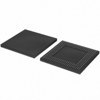
LPC3180FEL320/01,5 NXP Semiconductors, LPC3180FEL320/01,5 Datasheet - Page 21

LPC3180FEL320/01,5
Manufacturer Part Number
LPC3180FEL320/01,5
Description
IC ARM9 MCU 208MHZ 320-LFBGA
Manufacturer
NXP Semiconductors
Series
LPC3000r
Specifications of LPC3180FEL320/01,5
Package / Case
320-LFBGA
Core Processor
ARM9
Core Size
16/32-Bit
Speed
208MHz
Connectivity
EBI/EMI, I²C, MMC, SPI, UART/USART, USB OTG
Peripherals
DMA, PWM, WDT
Number Of I /o
55
Program Memory Type
ROMless
Ram Size
64K x 8
Voltage - Supply (vcc/vdd)
1.1 V ~ 3.3 V
Data Converters
A/D 3x10b
Oscillator Type
External
Operating Temperature
-40°C ~ 85°C
Processor Series
LPC31
Core
ARM926EJ-S
Data Bus Width
32 bit
Maximum Clock Frequency
208 MHz
Operating Supply Voltage
1.8 V / 3V
Maximum Operating Temperature
+ 85 C
Mounting Style
SMD/SMT
3rd Party Development Tools
MDK-ARM, RL-ARM, ULINK2
Development Tools By Supplier
OM10096
Minimum Operating Temperature
- 40 C
Package
320LFBGA
Device Core
ARM926EJ-S
Family Name
LPC3100
Maximum Speed
208 MHz
Number Of Programmable I/os
55
Interface Type
I2C/SPI/UART/USB
On-chip Adc
3-chx10-bit
Number Of Timers
2
Lead Free Status / RoHS Status
Lead free / RoHS Compliant
For Use With
622-1018 - EVAL KIT FOR LP3180568-4063 - KIT DEV LPC3180568-4062 - DEBUGGER J-LINK JTAG568-4061 - DEBUGGER U-LINK2 JTAG FOR NXP
Eeprom Size
-
Program Memory Size
-
Lead Free Status / Rohs Status
Lead free / RoHS Compliant
Other names
568-4529
935286983551
935286983551
Available stocks
Company
Part Number
Manufacturer
Quantity
Price
Company:
Part Number:
LPC3180FEL320/01,5
Manufacturer:
NXP Semiconductors
Quantity:
10 000
NXP Semiconductors
LPC3180_2
Preliminary data sheet
6.13.2.1 Features
6.14.1 Features
6.15.1 Features
6.14 I
6.15 SPI serial I/O controller
There are two I
only implementation supporting the 400 kHz I
slave addressing. Each has a four word FIFO for both transmit and receive. An interrupt
signal is available from each block.
The LPC3180 has two Serial Peripheral Interfaces (SPI). The SPI is a 3-wire serial
interface that is able to interface with a large range of serial peripheral or memory devices
(SPI mode 0 to 3 compatible slave devices).
Only a single master and a single slave can communicate on the interface during a given
data transfer. During a data transfer the master always sends a byte of data to the slave,
and the slave always sends a byte of data to the master. The SPI implementation on the
LPC3180 does not support operation as a slave.
2
•
•
•
•
•
•
•
•
•
•
•
•
•
•
•
•
•
•
C-bus serial I/O controller
Each high-speed UART has 64 byte Receive and Transmit FIFOs.
Receiver FIFO trigger points at 1 B, 4 B, 8 B, 16 B, 32 B, and 48 B.
Transmitter FIFO trigger points at 0 B, 4 B, and 8 B.
Each high-speed UART has an internal baud rate generator.
The high-speed UARTs are designed to support data rates of (2400, 4800, 9600,
19200, 38400, 57600, 115200, 230400, 460800, 921600) bit/s.
Each UART includes an internal loopback mode.
The two I
Single Master mode only.
Programmable clock to allow adjustment of I
Bidirectional data transfer.
Serial clock synchronization allows devices with different bit rates to communicate via
one serial bus.
Serial clock synchronization can be used as a handshake mechanism to suspend and
resume serial transfer.
Supports slaves compatible with SPI modes 0 to 3.
Half duplex synchronous transfers.
DMA support for data transmit and receive.
1-bit to 16-bit word length.
Choice of LSB or MSB first data transmission.
64
Bit rates up to 52 Mbit/s.
16-bit input or output FIFO.
2
C-bus blocks are standard I
2
C-bus interfaces in the LPC3180. The blocks for the I
Rev. 02 — 15 February 2007
16/32-bit ARM microcontroller with external memory interface
2
C-bus compliant interfaces that may be used in
2
C-bus mode and lower rates, with 7-bit
2
C-bus transfer rates.
2
C-bus are a master
LPC3180
© NXP B.V. 2007. All rights reserved.
21 of 36


