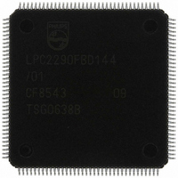
LPC2290FBD144/01,5 NXP Semiconductors, LPC2290FBD144/01,5 Datasheet - Page 8

LPC2290FBD144/01,5
Manufacturer Part Number
LPC2290FBD144/01,5
Description
IC ARM7 MCU RAM 16K 144-LQFP
Manufacturer
NXP Semiconductors
Series
LPC2200r
Datasheet
1.LPC2290FBD144015.pdf
(41 pages)
Specifications of LPC2290FBD144/01,5
Package / Case
144-LQFP
Core Processor
ARM7
Core Size
16/32-Bit
Speed
60MHz
Connectivity
CAN, EBI/EMI, I²C, Microwire, SPI, SSI, SSP, UART/USART
Peripherals
PWM, WDT
Number Of I /o
76
Program Memory Type
ROMless
Ram Size
64K x 8
Voltage - Supply (vcc/vdd)
1.65 V ~ 3.6 V
Data Converters
A/D 8x10b
Oscillator Type
Internal
Operating Temperature
-40°C ~ 85°C
Processor Series
LPC22
Core
ARM7TDMI-S
Data Bus Width
16 bit, 32 bit
Data Ram Size
64 KB
Interface Type
CAN/I2C/SPI/UART
Maximum Clock Frequency
72 MHz
Number Of Programmable I/os
76
Number Of Timers
2
Operating Supply Voltage
3.3 V
Maximum Operating Temperature
+ 85 C
Mounting Style
SMD/SMT
3rd Party Development Tools
MDK-ARM, RL-ARM, ULINK2
Minimum Operating Temperature
- 40 C
On-chip Adc
8-ch x 10-bit
Package
144LQFP
Device Core
ARM7TDMI-S
Family Name
LPC2000
Maximum Speed
72 MHz
Lead Free Status / RoHS Status
Lead free / RoHS Compliant
For Use With
OM10091 - KIT DEV PHYCORE-ARM7/LPC2220568-1757 - BOARD EVAL FOR LPC220X ARM MCU
Eeprom Size
-
Program Memory Size
-
Lead Free Status / Rohs Status
Lead free / RoHS Compliant
Other names
568-4013
935282079551
LPC2290FBD144/01-S
935282079551
LPC2290FBD144/01-S
Available stocks
Company
Part Number
Manufacturer
Quantity
Price
Company:
Part Number:
LPC2290FBD144/01,5
Manufacturer:
NXP Semiconductors
Quantity:
10 000
NXP Semiconductors
Table 3.
LPC2290_3
Product data sheet
Symbol
P1.0/CS0
P1.1/OE
P1.16/
TRACEPKT0
P1.17/
TRACEPKT1
P1.18/
TRACEPKT2
P1.19/
TRACEPKT3
P1.20/
TRACESYNC
P1.21/
PIPESTAT0
P1.22/
PIPESTAT1
P1.23/
PIPESTAT2
P1.24/
TRACECLK
P1.25/EXTIN0
P1.26/RTCK
P1.27/TDO
P1.28/TDI
P1.29/TCK
P1.30/TMS
Pin description
Pin
91
90
34
24
15
7
102
95
86
82
70
60
52
144
140
126
113
[5]
[5]
[5]
[5]
[5]
[5]
[5]
[5]
[5]
[5]
[5]
[5]
[5]
[5]
[5]
[5]
[5]
…continued
Type
I/O
O
I/O
O
I/O
O
I/O
O
I/O
O
I/O
O
I/O
O
I/O
O
I/O
O
I/O
O
I/O
O
I/O
I
I/O
I/O
I/O
O
I/O
I
I/O
I
I/O
I
Description
P1.0 — General purpose digital input/output pin.
CS0 — LOW-active Chip Select 0 signal.
P1.1 — General purpose digital input/output pin.
OE — LOW-active Output Enable signal.
P1.16 — General purpose digital input/output pin.
TRACEPKT0 — Trace Packet, bit 0. Standard I/O port with internal pull-up.
P1.17 — General purpose digital input/output pin.
TRACEPKT1 — Trace Packet, bit 1. Standard I/O port with internal pull-up.
P1.18 — General purpose digital input/output pin.
TRACEPKT2 — Trace Packet, bit 2. Standard I/O port with internal pull-up.
P1.19 — General purpose digital input/output pin.
TRACEPKT3 — Trace Packet, bit 3. Standard I/O port with internal pull-up.
P1.20 — General purpose digital input/output pin.
TRACESYNC — Trace Synchronization. Standard I/O port with internal
pull-up.
Note: LOW on this pin while RESET is LOW, enables pins P1[25:16] to
operate as Trace port after reset.
P1.21 — General purpose digital input/output pin.
PIPESTAT0 — Pipeline Status, bit 0. Standard I/O port with internal pull-up.
P1.22 — General purpose digital input/output pin.
PIPESTAT1 — Pipeline Status, bit 1. Standard I/O port with internal pull-up.
P1.23 — General purpose digital input/output pin.
PIPESTAT2 — Pipeline Status, bit 2. Standard I/O port with internal pull-up.
P1.24 — General purpose digital input/output pin.
TRACECLK — Trace Clock. Standard I/O port with internal pull-up.
P1.25 — General purpose digital input/output pin.
EXTIN0 — External Trigger Input. Standard I/O with internal pull-up.
P1.26 — General purpose digital input/output pin.
RTCK — Returned Test Clock output. Extra signal added to the JTAG port.
Assists debugger synchronization when processor frequency varies.
Bidirectional pin with internal pull-up.
Note: LOW on this pin while RESET is LOW, enables pins P1[31:26] to
operate as Debug port after reset.
P1.27 — General purpose digital input/output pin.
TDO — Test Data out for JTAG interface.
P1.28 — General purpose digital input/output pin.
TDI — Test Data in for JTAG interface.
P1.29 — General purpose digital input/output pin.
TCK — Test Clock for JTAG interface.
P1.30 — General purpose digital input/output pin.
TMS — Test Mode Select for JTAG interface.
(Bank 0 addresses range 0x8000 0000 to 0x80FF FFFF)
Rev. 03 — 16 November 2006
16/32-bit ARM microcontroller with external memory interface
LPC2290
© NXP B.V. 2006. All rights reserved.
8 of 41


