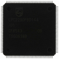
LPC2290FBD144/01,5 NXP Semiconductors, LPC2290FBD144/01,5 Datasheet - Page 12

LPC2290FBD144/01,5
Manufacturer Part Number
LPC2290FBD144/01,5
Description
IC ARM7 MCU RAM 16K 144-LQFP
Manufacturer
NXP Semiconductors
Series
LPC2200r
Datasheet
1.LPC2290FBD144015.pdf
(41 pages)
Specifications of LPC2290FBD144/01,5
Package / Case
144-LQFP
Core Processor
ARM7
Core Size
16/32-Bit
Speed
60MHz
Connectivity
CAN, EBI/EMI, I²C, Microwire, SPI, SSI, SSP, UART/USART
Peripherals
PWM, WDT
Number Of I /o
76
Program Memory Type
ROMless
Ram Size
64K x 8
Voltage - Supply (vcc/vdd)
1.65 V ~ 3.6 V
Data Converters
A/D 8x10b
Oscillator Type
Internal
Operating Temperature
-40°C ~ 85°C
Processor Series
LPC22
Core
ARM7TDMI-S
Data Bus Width
16 bit, 32 bit
Data Ram Size
64 KB
Interface Type
CAN/I2C/SPI/UART
Maximum Clock Frequency
72 MHz
Number Of Programmable I/os
76
Number Of Timers
2
Operating Supply Voltage
3.3 V
Maximum Operating Temperature
+ 85 C
Mounting Style
SMD/SMT
3rd Party Development Tools
MDK-ARM, RL-ARM, ULINK2
Minimum Operating Temperature
- 40 C
On-chip Adc
8-ch x 10-bit
Package
144LQFP
Device Core
ARM7TDMI-S
Family Name
LPC2000
Maximum Speed
72 MHz
Lead Free Status / RoHS Status
Lead free / RoHS Compliant
For Use With
OM10091 - KIT DEV PHYCORE-ARM7/LPC2220568-1757 - BOARD EVAL FOR LPC220X ARM MCU
Eeprom Size
-
Program Memory Size
-
Lead Free Status / Rohs Status
Lead free / RoHS Compliant
Other names
568-4013
935282079551
LPC2290FBD144/01-S
935282079551
LPC2290FBD144/01-S
Available stocks
Company
Part Number
Manufacturer
Quantity
Price
Company:
Part Number:
LPC2290FBD144/01,5
Manufacturer:
NXP Semiconductors
Quantity:
10 000
NXP Semiconductors
Table 3.
LPC2290_3
Product data sheet
Symbol
P3.20/A20
P3.21/A21
P3.22/A22
P3.23/A23/
XCLK
P3.24/CS3
P3.25/CS2
P3.26/CS1
P3.27/WE
P3.28/BLS3/
AIN7
P3.29/BLS2/
AIN6
P3.30/BLS1
P3.31/BLS0
TD1
RESET
XTAL1
XTAL2
V
V
SS
SSA
Pin description
Pin
45
44
41
40
36
35
30
29
28
27
97
96
22
135
142
141
3, 9, 26, 38,
54, 67, 79,
93, 103, 107,
111, 128
139
[5]
[5]
[5]
[5]
[5]
[5]
[5]
[5]
[2]
[4]
[4]
[4]
[5]
[6]
[7]
[7]
…continued
Type
I/O
O
I/O
O
I/O
O
I/O
I/O
O
I/O
O
I/O
O
I/O
O
I/O
O
I/O
O
I
I/O
O
I
I/O
O
I/O
O
O
I
I
O
I
I
Description
P3.20 — General purpose digital input/output pin.
A20 — External memory address line 20.
P3.21 — General purpose digital input/output pin.
A21 — External memory address line 21.
P3.22 — General purpose digital input/output pin.
A22 — External memory address line 22.
P3.23 — General purpose digital input/output pin.
A23 — External memory address line 23.
XCLK — Clock output.
P3.24 — General purpose digital input/output pin.
CS3 — LOW-active Chip Select 3 signal.
(Bank 3 addresses range 0x8300 0000 to 0x83FF FFFF)
P3.25 — General purpose digital input/output pin.
CS2 — LOW-active Chip Select 2 signal.
(Bank 2 addresses range 0x8200 0000 to 0x82FF FFFF)
P3.26 — General purpose digital input/output pin.
CS1 — LOW-active Chip Select 1 signal.
(Bank 1 addresses range 0x8100 0000 to 0x81FF FFFF)
P3.27 — General purpose digital input/output pin.
WE — LOW-active Write enable signal.
P3.28 — General purpose digital input/output pin.
BLS3 — LOW-active Byte Lane Select signal (Bank 3).
AIN7 — ADC, input 7. This analog input is always connected to its pin.
P3.29 — General purpose digital input/output pin.
BLS2 — LOW-active Byte Lane Select signal (Bank 2).
AIN6 — ADC, input 6. This analog input is always connected to its pin.
P3.30 — General purpose digital input/output pin.
BLS1 — LOW-active Byte Lane Select signal (Bank 1).
P3.31 — General purpose digital input/output pin.
BLS0 — LOW-active Byte Lane Select signal (Bank 0).
TD1: CAN1 transmitter output.
External Reset input: A LOW on this pin resets the device, causing I/O ports
and peripherals to take on their default states, and processor execution to
begin at address 0. TTL with hysteresis, 5 V tolerant.
Input to the oscillator circuit and internal clock generator circuits.
Output from the oscillator amplifier.
Ground: 0 V reference.
Analog ground: 0 V reference. This should nominally be the same voltage
as V
Rev. 03 — 16 November 2006
SS
16/32-bit ARM microcontroller with external memory interface
, but should be isolated to minimize noise and error.
LPC2290
© NXP B.V. 2006. All rights reserved.
12 of 41


