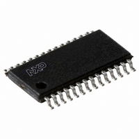
P89LPC935FDH,529 NXP Semiconductors, P89LPC935FDH,529 Datasheet - Page 53

P89LPC935FDH,529
Manufacturer Part Number
P89LPC935FDH,529
Description
IC 80C51 MCU FLASH 8K 28-TSSOP
Manufacturer
NXP Semiconductors
Series
LPC900r
Datasheet
1.P89LPC936FDH518.pdf
(77 pages)
Specifications of P89LPC935FDH,529
Program Memory Type
FLASH
Program Memory Size
8KB (8K x 8)
Package / Case
28-TSSOP
Core Processor
8051
Core Size
8-Bit
Speed
12MHz
Connectivity
I²C, SPI, UART/USART
Peripherals
Brown-out Detect/Reset, LED, POR, PWM, WDT
Number Of I /o
26
Eeprom Size
512 x 8
Ram Size
768 x 8
Voltage - Supply (vcc/vdd)
2.4 V ~ 3.6 V
Data Converters
A/D 8x8b; D/A 2x8b
Oscillator Type
Internal
Operating Temperature
-40°C ~ 85°C
Processor Series
P89LPC9x
Core
80C51
Data Bus Width
8 bit
Data Ram Size
768 B
Interface Type
I2C/SPI/UART
Maximum Clock Frequency
18 MHz
Number Of Programmable I/os
26
Number Of Timers
2
Operating Supply Voltage
2.4 V to 3.6 V
Maximum Operating Temperature
+ 85 C
Mounting Style
SMD/SMT
3rd Party Development Tools
PK51, CA51, A51, ULINK2
Minimum Operating Temperature
- 40 C
On-chip Adc
8-ch x 8-bit
Package
28TSSOP
Device Core
80C51
Family Name
89LP
Maximum Speed
18 MHz
Lead Free Status / RoHS Status
Lead free / RoHS Compliant
For Use With
OM11004 - KIT IAR KICKSTART LPC935622-1014 - BOARD FOR LPC9XX TSSOP622-1008 - BOARD FOR LPC9103 10-HVSON622-1006 - SOCKET ADAPTER BOARDMCB900K - BOARD PROTOTYPE NXP 89LPC9EPM900K - EMULATOR/PROGRAMMER NXP P89LPC9568-4000 - DEMO BOARD SPI/I2C TO DUAL UART568-3510 - DEMO BOARD SPI/I2C TO UART622-1002 - USB IN-CIRCUIT PROG LPC9XX568-1759 - EMULATOR DEBUGGER/PROGRMMR LPC9X568-1758 - BOARD EVAL FOR LPC93X MCU FAMILY
Lead Free Status / Rohs Status
Lead free / RoHS Compliant
Other names
568-1288-5
935274646529
P89LPC935FDH-S
935274646529
P89LPC935FDH-S
NXP Semiconductors
P89LPC933_934_935_936
Product data sheet
9.4.1 Fixed channel, single conversion mode
9.3 Block diagram
9.4 A/D operating modes
A single input channel can be selected for conversion. A single conversion will be
performed and the result placed in the result register which corresponds to the selected
input channel. An interrupt, if enabled, will be generated after the conversion completes.
Fig 23. ADC block diagram
8-bit conversion time of ≥3.9 μs at an A/D clock of 3.3 MHz.
Interrupt or polled operation.
Boundary limits interrupt.
DAC output to a port pin with high output impedance.
Clock divider.
Power-down mode.
Start immediately.
Edge triggered.
Dual start immediately (P89LPC935/936).
All information provided in this document is subject to legal disclaimers.
INPUT
INPUT
MUX
MUX
Rev. 8 — 12 January 2011
8-bit microcontroller with accelerated two-clock 80C51 core
P89LPC933/934/935/936
comp
comp
+
–
+
–
DAC1
DAC0
CCLK
SAR
SAR
8
8
© NXP B.V. 2011. All rights reserved.
CONTROL
LOGIC
002aab080
53 of 77


