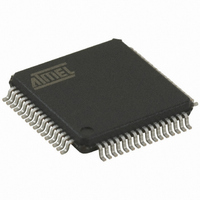
AT89C5122D-RDTUM Atmel, AT89C5122D-RDTUM Datasheet - Page 104

AT89C5122D-RDTUM
Manufacturer Part Number
AT89C5122D-RDTUM
Description
IC 8051 MCU FLASH 32K 64VQFP
Manufacturer
Atmel
Series
89Cr
Datasheet
1.AT89C5122D-PSTUM.pdf
(208 pages)
Specifications of AT89C5122D-RDTUM
Core Processor
8051
Core Size
8-Bit
Speed
48MHz
Connectivity
SmartCard, SPI, UART/USART, USB
Peripherals
LED, POR, WDT
Number Of I /o
46
Program Memory Size
32KB (32K x 8)
Program Memory Type
FLASH
Ram Size
768 x 8
Voltage - Supply (vcc/vdd)
3 V ~ 5.5 V
Oscillator Type
Internal
Operating Temperature
-40°C ~ 85°C
Package / Case
64-TQFP, 64-VQFP
For Use With
AT89OCD-01 - USB EMULATOR FOR AT8XC51 MCUAT89STK-10 - KIT EVAL APPL MASS STORAGEAT89STK-03 - KIT STARTER FOR MCU AT8XC5122/23
Lead Free Status / RoHS Status
Lead free / RoHS Compliant
Eeprom Size
-
Data Converters
-
- Current page: 104 of 208
- Download datasheet (3Mb)
Bulk/Interrupt IN Transactions
in Ping-Pong Mode
104
AT83R5122, AT8xC5122/23
Figure 57. Bulk / Interrupt IN transactions in Ping-Pong mode
An endpoint will be first enabled and configured before being able to send Bulk or Inter-
rupt packets.
The firmware will fill the FIFO bank 0 with the data to be sent and set the TXRDY bit in
the UEPSTAX register to allow the USB controller to send the data stored in FIFO at the
next IN request concerning the endpoint. The FIFO banks are automatically switched,
and the firmware can immediately write into the endpoint FIFO bank 1.
When the IN packet concerning the bank 0 has been sent and acknowledged by the
Host, the TXCMPL bit is set by the USB controller. This triggers a USB interrupt if
enabled. The firmware will clear the TXCMPL bit before filling the endpoint FIFO bank 0
with new data. The FIFO banks are then automatically switched.
When the IN packet concerning the bank 1 has been sent and acknowledged by the
Host, the TXCMPL bit is set by the USB controller. This triggers a USB interrupt if
enabled. The firmware will clear the TXCMPL bit before filling the endpoint FIFO bank 1
with new data.
The bank switch is performed by the USB controller each time the TXRDY bit is set by
the firmware. Until the TXRDY bit has been set by the firmware for an endpoint bank,
the USB controller will answer a NAK handshake for each IN requests concerning this
bank.
Note that in the example above, the firmware clears the Transmit Complete bit (TXC-
MPL) before setting the Transmit Ready bit (TXRDY). This is done in order to avoid the
firmware to clear at the same time the TXCMPL bit for bank 0 and the bank 1.
The firmware will never write more bytes than supported by the endpoint FIFO.
HOST
IN
IN
IN
IN
ACK
ACK
ACK
DATA0 (n Bytes)
DATA1 (m Bytes)
DATA0 (p Bytes)
NACK
UFI
TXCMPL
TXCMPL
Endpoint FIFO Bank 0 - Write Byte 1
Endpoint FIFO Bank 0 - Write Byte 2
Endpoint FIFO Bank 0 - Write Byte n
Endpoint FIFO Bank 1 - Write Byte 1
Endpoint FIFO Bank 1 - Write Byte 2
Endpoint FIFO Bank 1 - Write Byte m
Endpoint FIFO Bank 0 - Write Byte 1
Endpoint FIFO Bank 0 - Write Byte 2
Endpoint FIFO Bank 0 - Write Byte p
Endpoint FIFO Bank 1 - Write Byte 1
C51
Clear TXCMPL
Clear TXCMPL
Set TXRDY
Set TXRDY
Set TXRDY
4202F–SCR–07/2008
Related parts for AT89C5122D-RDTUM
Image
Part Number
Description
Manufacturer
Datasheet
Request
R

Part Number:
Description:
IC 8051 MCU 32K CRAM USB 64-VQFP
Manufacturer:
Atmel
Datasheet:

Part Number:
Description:
IC 8051 MCU W/SMART CARD 64VQFP
Manufacturer:
Atmel
Datasheet:

Part Number:
Description:
IC 8051 MCU FLASH 32K 64QFN
Manufacturer:
Atmel
Datasheet:

Part Number:
Description:
IC MCU 80C51 W/SMART CARD 64VQFP
Manufacturer:
Atmel
Datasheet:

Part Number:
Description:
IC 8051 MCU FLASH 32K 28PLCC
Manufacturer:
Atmel
Datasheet:

Part Number:
Description:
MICROCONTROLLER WITH USB AND SMART CARD READER INTERFACES
Manufacturer:
ATMEL [ATMEL Corporation]
Datasheet:

Part Number:
Description:
KIT STARTER FOR MCU AT8XC5122/23
Manufacturer:
Atmel
Datasheet:

Part Number:
Description:
IC MICRO CTRL 24MHZ 44TQFP
Manufacturer:
Atmel
Datasheet:

Part Number:
Description:
IC MICRO CTRL 24MHZ 44PLCC
Manufacturer:
Atmel
Datasheet:

Part Number:
Description:
IC MICRO CTRL 24MHZ 44PLCC
Manufacturer:
Atmel
Datasheet:

Part Number:
Description:
IC MICRO CTRL 24MHZ 40DIP
Manufacturer:
Atmel
Datasheet:


