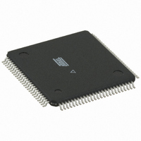
ATMEGA3290P-20AU Atmel, ATMEGA3290P-20AU Datasheet - Page 239

ATMEGA3290P-20AU
Manufacturer Part Number
ATMEGA3290P-20AU
Description
IC MCU 32K 4X40 LCD CTRL 100TQFP
Manufacturer
Atmel
Series
AVR® ATmegar
Specifications of ATMEGA3290P-20AU
Core Processor
AVR
Core Size
8-Bit
Speed
20MHz
Connectivity
SPI, UART/USART, USI
Peripherals
Brown-out Detect/Reset, LCD, POR, PWM, WDT
Number Of I /o
69
Program Memory Size
32KB (16K x 16)
Program Memory Type
FLASH
Eeprom Size
1K x 8
Ram Size
2K x 8
Voltage - Supply (vcc/vdd)
2.7 V ~ 5.5 V
Data Converters
A/D 8x10b
Oscillator Type
Internal
Operating Temperature
-40°C ~ 85°C
Package / Case
100-TQFP, 100-VQFP
Processor Series
ATMEGA32x
Core
AVR8
Data Bus Width
8 bit
Data Ram Size
2 KB
Interface Type
SPI, USART, USI
Maximum Clock Frequency
20 MHz
Number Of Programmable I/os
69
Number Of Timers
3
Maximum Operating Temperature
+ 85 C
Mounting Style
SMD/SMT
3rd Party Development Tools
EWAVR, EWAVR-BL
Development Tools By Supplier
ATAVRDRAGON, ATSTK500, ATSTK600, ATAVRISP2, ATAVRONEKIT
Minimum Operating Temperature
- 40 C
On-chip Adc
10 bit, 8 Channel
Package
100TQFP
Device Core
AVR
Family Name
ATmega
Maximum Speed
20 MHz
Operating Supply Voltage
3.3|5 V
Controller Family/series
AVR MEGA
No. Of I/o's
69
Eeprom Memory Size
1KB
Ram Memory Size
2KB
Cpu Speed
20MHz
Rohs Compliant
Yes
For Use With
ATSTK600-TQFP100 - STK600 SOCKET/ADAPTER 100-TQFP770-1007 - ISP 4PORT ATMEL AVR MCU SPI/JTAG770-1005 - ISP 4PORT FOR ATMEL AVR MCU JTAG770-1004 - ISP 4PORT FOR ATMEL AVR MCU SPIATAVRISP2 - PROGRAMMER AVR IN SYSTEMATSTK504 - STARTER KIT AVR EXP MOD 100P LCDATJTAGICE2 - AVR ON-CHIP D-BUG SYSTEM
Lead Free Status / RoHS Status
Lead free / RoHS Compliant
Other names
ATMEGA3290P-16AU
ATMEGA3290P-16AU
ATMEGA3290P-16AU
Available stocks
Company
Part Number
Manufacturer
Quantity
Price
- Current page: 239 of 427
- Download datasheet (9Mb)
23.4.2
23.4.3
8021G–AVR–03/11
Updating the LCD
Disabling the LCD
Display memory (LCDDR0, LCDDR1,...), LCD Blanking (LCDBL), Low power waveform
(LCDAB) and contrast control (LCDCCR) are latched prior to every new frame. There are no
restrictions on writing these LCD Register locations, but an LCD data update may be split
between two frames if data are latched while an update is in progress. To avoid this, an interrupt
routine can be used to update Display memory, LCD Blanking, Low power waveform, and con-
trast control, just after data are latched.
In the example below we assume SEG10 and COM1 and SEG4 in COM0 are the only segments
changed from frame to frame. Data are stored in r20 and r21 for simplicity
Note:
In some application it may be necessary to disable the LCD. This is the case if the MCU enters
Power-down mode where no clock source is present.
The LCD should be completely discharged before being disabled. No DC voltage should be left
across any segment. The best way to achieve this is to use the LCD Blanking feature that drives
all segment pins and common pins to GND.
When the LCD is disabled, port function is activated again. Therefore, the user must check that
port pins connected to a LCD terminal are either tri-state or output low (sink).
Assembly Code Example
C Code Example
LCD_update:
Void LCD_update(unsigned char data1, data2);
{
}
; LCD Blanking and Low power waveform are unchanged.
; Update Display memory.
sts
sts
ret
/* LCD Blanking and Low power waveform are unchanged. */
/* Update Display memory. */
LCDDR0 = data1;
LCDDR6 = data2;
1. See
LCDDR0, r20
LCDDR6, r21
”About Code Examples” on page
(1)
(1)
9.
ATmega329P/3290P
239
Related parts for ATMEGA3290P-20AU
Image
Part Number
Description
Manufacturer
Datasheet
Request
R

Part Number:
Description:
Manufacturer:
Atmel Corporation
Datasheet:

Part Number:
Description:
IC AVR MCU 32K 16MHZ 100TQFP
Manufacturer:
Atmel
Datasheet:

Part Number:
Description:
IC AVR MCU 32K 16MHZ 100TQFP
Manufacturer:
Atmel
Datasheet:

Part Number:
Description:
MCU AVR 32K FLASH 16MHZ 64TQFP
Manufacturer:
Atmel
Datasheet:

Part Number:
Description:
Atmega3290 Avr 8-bit Microcontroller With In-system Programmable Flash
Manufacturer:
ATMEL Corporation
Datasheet:

Part Number:
Description:
Manufacturer:
Atmel Corporation
Datasheet:

Part Number:
Description:
IC AVR MCU 32K 16MHZ 64TQFP
Manufacturer:
Atmel
Datasheet:

Part Number:
Description:
IC AVR MCU 32K 16MHZ 64-QFN
Manufacturer:
Atmel
Datasheet:

Part Number:
Description:
IC AVR MCU 32K 16MHZ 64TQFP
Manufacturer:
Atmel
Datasheet:

Part Number:
Description:
IC AVR MCU 32K 16MHZ 64-QFN
Manufacturer:
Atmel
Datasheet:

Part Number:
Description:
MCU AVR 32K FLASH 16MHZ 64TQFP
Manufacturer:
Atmel
Datasheet:

Part Number:
Description:
MCU AVR 32K FLASH 16MHZ 64QFN
Manufacturer:
Atmel
Datasheet:

Part Number:
Description:
DEV KIT FOR AVR/AVR32
Manufacturer:
Atmel
Datasheet:

Part Number:
Description:
INTERVAL AND WIPE/WASH WIPER CONTROL IC WITH DELAY
Manufacturer:
ATMEL Corporation
Datasheet:


