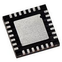
PIC18LF27J53-I/ML Microchip Technology, PIC18LF27J53-I/ML Datasheet - Page 4

PIC18LF27J53-I/ML
Manufacturer Part Number
PIC18LF27J53-I/ML
Description
IC PIC MCU 128KB FLASH 28QFN
Manufacturer
Microchip Technology
Series
PIC® XLP™ 18Fr
Datasheets
1.PIC18LF24J10-ISS.pdf
(32 pages)
2.PIC18F26J13-ISS.pdf
(496 pages)
3.PIC18F26J53-ISS.pdf
(586 pages)
4.PIC18F26J53-ISS.pdf
(12 pages)
Specifications of PIC18LF27J53-I/ML
Core Size
8-Bit
Program Memory Size
128KB (64K x 16)
Core Processor
PIC
Speed
48MHz
Connectivity
I²C, LIN, SPI, UART/USART, USB
Peripherals
Brown-out Detect/Reset, POR, PWM, WDT
Number Of I /o
22
Program Memory Type
FLASH
Ram Size
3.8K x 8
Voltage - Supply (vcc/vdd)
2 V ~ 2.75 V
Data Converters
A/D 10x10b/12b
Oscillator Type
Internal
Operating Temperature
-40°C ~ 85°C
Package / Case
*
Controller Family/series
PIC18
Cpu Speed
48MHz
Digital Ic Case Style
QFN
Supply Voltage Range
1.8V To 3.6V
Embedded Interface Type
I2C, SPI, USART
Rohs Compliant
Yes
Lead Free Status / RoHS Status
Lead free / RoHS Compliant
Eeprom Size
-
Lead Free Status / RoHS Status
Lead free / RoHS Compliant, Lead free / RoHS Compliant
Available stocks
Company
Part Number
Manufacturer
Quantity
Price
Company:
Part Number:
PIC18LF27J53-I/ML
Manufacturer:
ATMEL
Quantity:
101
PIC18F2XJXX/4XJXX FAMILY
2.1.1
PIC18FXXJXX devices have an internal core voltage
regulator. On these devices (“PIC18F” in the part num-
ber), the regulator is always enabled. The regulator
input is taken from the microcontroller V
output of the regulator is supplied to the V
pin. On these devices, this pin simultaneously serves
as both the regulator output and the microcontroller
core power input pin. For these devices, the
V
nothing else.
PIC18LFXXJXX devices do not have an internal core
voltage regulator. On these devices (“PIC18LF” in the
part number), power must be externally supplied to
both V
Whether or not the regulator is used, it is always good
design practice to have sufficient capacitance on all
supply pins. Examples are shown in Figure 2-3.
The specifications for core voltage and capacitance are
listed in Section 6.0 “AC/DC Characteristics Timing
Requirements for Program/Verify Test Mode”.
FIGURE 2-3:
DS39687E-page 4
DDCORE
PIC18LF2XJXX/4XJXX Devices (Regulator Disabled)
PIC18F2XJXX/4XJXX Devices (Regulator Enabled)
(V
(V
DD
DD
DD
/V
and V
= V
≥ V
CAP
PIC18F2XJXX/4XJXX/
LF2XJXX/LF4XJXX DEVICES AND
THE ON-CHIP VOLTAGE
REGULATOR
C
DDCORE
DDCORE
F
3.3V
DDCORE
pin should be tied to a capacitor and
2.5V
2.5V
)
)
3.3V
V
V
V
CONNECTIONS FOR THE
ON-CHIP REGULATOR
PIC18F2XJXX/4XJXX
/V
DD
DDCORE
SS
CAP
PIC18LF2XJXX/4XJXX
PIC18LF2XJXX/4XJXX
V
V
V
V
V
V
DD
DDCORE
SS
DD
DDCORE
SS
.
/V
CAP
/V
/V
CAP
CAP
DDCORE
DD
pins. The
/V
CAP
2.2
The PIC18F2XJXX/4XJXX family of devices offers
program memory sizes of 16, 32, 64 and 128 Kbytes.
The memory sizes for different members of the family
are shown in Table 2-2. The overall memory maps for
all the devices are shown in Figure 2-4.
TABLE 2-2:
For purposes of code protection, the program memory
for every device is treated as a single block. Enabling
code protection, thus protects the entire code memory,
and not individual segments.
*
PIC18F24J10
PIC18F44J10
PIC18F24J11
PIC18F44J11
PIC18F24J50
PIC18F44J50
PIC18F25J10
PIC18F45J10
PIC18F25J11
PIC18F45J11
PIC18F25J50
PIC18F45J50
PIC18F26J11
PIC18F46J11
PIC18F26J13
PIC18F46J13
PIC18F26J50
PIC18F46J50
PIC18F26J53
PIC18F46J53
PIC18F27J13
PIC18F47J13
PIC18F27J53
PIC18F47J53
Includes PIC18F and PIC18LF devices.
Device*
Memory Maps
PROGRAM MEMORY SIZES
FOR PIC18F2XJXX/4XJXX
FAMILY DEVICES
Program
(Kbytes)
Memory
© 2009 Microchip Technology Inc.
128
16
32
64
Location of Flash
1FFF8h:1FFFFh
Configuration
FFF8h:FFFFh
3FF8h:3FFFh
7FF8h:7FFFh
Words


