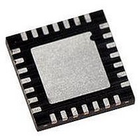
PIC18LF27J53-I/ML Microchip Technology, PIC18LF27J53-I/ML Datasheet - Page 16

PIC18LF27J53-I/ML
Manufacturer Part Number
PIC18LF27J53-I/ML
Description
IC PIC MCU 128KB FLASH 28QFN
Manufacturer
Microchip Technology
Series
PIC® XLP™ 18Fr
Datasheets
1.PIC18LF24J10-ISS.pdf
(32 pages)
2.PIC18F26J13-ISS.pdf
(496 pages)
3.PIC18F26J53-ISS.pdf
(586 pages)
4.PIC18F26J53-ISS.pdf
(12 pages)
Specifications of PIC18LF27J53-I/ML
Core Size
8-Bit
Program Memory Size
128KB (64K x 16)
Core Processor
PIC
Speed
48MHz
Connectivity
I²C, LIN, SPI, UART/USART, USB
Peripherals
Brown-out Detect/Reset, POR, PWM, WDT
Number Of I /o
22
Program Memory Type
FLASH
Ram Size
3.8K x 8
Voltage - Supply (vcc/vdd)
2 V ~ 2.75 V
Data Converters
A/D 10x10b/12b
Oscillator Type
Internal
Operating Temperature
-40°C ~ 85°C
Package / Case
*
Controller Family/series
PIC18
Cpu Speed
48MHz
Digital Ic Case Style
QFN
Supply Voltage Range
1.8V To 3.6V
Embedded Interface Type
I2C, SPI, USART
Rohs Compliant
Yes
Lead Free Status / RoHS Status
Lead free / RoHS Compliant
Eeprom Size
-
Lead Free Status / RoHS Status
Lead free / RoHS Compliant, Lead free / RoHS Compliant
Available stocks
Company
Part Number
Manufacturer
Quantity
Price
Company:
Part Number:
PIC18LF27J53-I/ML
Manufacturer:
ATMEL
Quantity:
101
PIC18F2XJXX/4XJXX FAMILY
4.0
4.1
Code memory is accessed one byte at a time via the
4-bit command, ‘1001’ (table read, post-increment).
The contents of memory pointed to by the Table Pointer
(TBLPTRU:TBLPTRH:TBLPTRL) are serially output on
PGD.
The 4-bit command is shifted in LSb first. The read is
executed during the next 8 clocks, then shifted out on
PGD during the last 8 clocks, LSb to MSb. A delay of
TABLE 4-1:
FIGURE 4-1:
DS39687E-page 16
Step 1: Set Table Pointer.
Step 2: Read memory and then shift out on PGD, LSb to MSb.
Command
PGC
PGD
0000
0000
0000
0000
0000
0000
1001
4-Bit
READING THE DEVICE
Read Code Memory
1
1
2
0E <Addr[21:16]>
6E F8
0E <Addr[15:8]>
6E F7
0E <Addr[7:0]>
6E F6
00 00
0
READ CODE MEMORY SEQUENCE
3
0
Data Payload
TABLE READ, POST-INCREMENT INSTRUCTION TIMING (1001)
4
1
P5
PGD = Input
1
2
3
MOVLW Addr[21:16]
MOVWF TBLPTRU
MOVLW <Addr[15:8]>
MOVWF TBLPTRH
MOVLW <Addr[7:0]>
MOVWF TBLPTRL
TBLRD *+
4
5
6
7
8
P6
P6 must be introduced after the falling edge of the 8th
PGC of the operand to allow PGD to transition from an
input to an output. During this time, PGC must be held
low (see Figure 4-1). This operation also increments
the Table Pointer by one, pointing to the next byte in
code memory for the next read.
This technique will work to read any memory in the
000000h to 3FFFFFh address space, so it also applies
to reading the Configuration registers.
9
LSb
P14
10
1
11
Core Instruction
2
PGD = Output
12
Shift Data Out
3
13
4
14
5
15
6
© 2009 Microchip Technology Inc.
16
MSb
P5A
Fetch Next 4-Bit Command
1
PGD = Input
n
2
n
3
n
4
n


