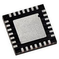
PIC18LF27J53-I/ML Microchip Technology, PIC18LF27J53-I/ML Datasheet - Page 21

PIC18LF27J53-I/ML
Manufacturer Part Number
PIC18LF27J53-I/ML
Description
IC PIC MCU 128KB FLASH 28QFN
Manufacturer
Microchip Technology
Series
PIC® XLP™ 18Fr
Datasheets
1.PIC18LF24J10-ISS.pdf
(32 pages)
2.PIC18F26J13-ISS.pdf
(496 pages)
3.PIC18F26J53-ISS.pdf
(586 pages)
4.PIC18F26J53-ISS.pdf
(12 pages)
Specifications of PIC18LF27J53-I/ML
Core Size
8-Bit
Program Memory Size
128KB (64K x 16)
Core Processor
PIC
Speed
48MHz
Connectivity
I²C, LIN, SPI, UART/USART, USB
Peripherals
Brown-out Detect/Reset, POR, PWM, WDT
Number Of I /o
22
Program Memory Type
FLASH
Ram Size
3.8K x 8
Voltage - Supply (vcc/vdd)
2 V ~ 2.75 V
Data Converters
A/D 10x10b/12b
Oscillator Type
Internal
Operating Temperature
-40°C ~ 85°C
Package / Case
*
Controller Family/series
PIC18
Cpu Speed
48MHz
Digital Ic Case Style
QFN
Supply Voltage Range
1.8V To 3.6V
Embedded Interface Type
I2C, SPI, USART
Rohs Compliant
Yes
Lead Free Status / RoHS Status
Lead free / RoHS Compliant
Eeprom Size
-
Lead Free Status / RoHS Status
Lead free / RoHS Compliant, Lead free / RoHS Compliant
Available stocks
Company
Part Number
Manufacturer
Quantity
Price
Company:
Part Number:
PIC18LF27J53-I/ML
Manufacturer:
ATMEL
Quantity:
101
TABLE 5-5:
© 2009 Microchip Technology Inc.
CPDIV<1:0>
IESO
FCMEN
LPT1OSC
T1DIG
FOSC<2:0>
WDTPS<3:0>
Note 1: The Configuration bits can only be programmed indirectly by programming the Flash Configuration Word.
Bit Name
2: The Configuration bits are reset to ‘1’ only on V
3: These bits are not implemented in PIC18F46J11 family devices.
4: Once this bit is cleared, all the Configuration registers which reside in the last page are also protected. To disable code
(3)
protection, perform an ICSP™ Bulk Erase operation.
PIC18F46J11 AND PIC18F46J50 FAMILY DEVICES: BIT DESCRIPTIONS (CONTINUED)
CONFIG2H
CONFIG2L
CONFIG2L
CONFIG2L
CONFIG2L
CONFIG2L
Configuration
CONFIG1H
Words
(1,2)
(1,2)
(1,2)
(1,2)
(1,2)
(1,2)
CPU System Clock Selection bits
11 = No CPU system clock divide
10 = CPU system clock divided by 2
01 = CPU system clock divided by 3
00 = CPU system clock divided by 6
Two-Speed Start-up (Internal/External Oscillator Switchover) Control bit
1 = Oscillator Switchover mode enabled
0 = Oscillator Switchover mode disabled
Fail-Safe Clock Monitor Enable bit
1 = Fail-Safe Clock Monitor enabled
0 = Fail-Safe Clock Monitor disabled
Low-Power Timer1 Oscillator Enable bit
1 = Timer1 oscillator configured for low-power operation
0 = Timer1 oscillator configured for higher power operation
Secondary Clock Source T1OSCEN Enforcement bit
1 = Secondary oscillator clock source may be selected (OSCCON <1:0> = 01)
0 = Secondary oscillator clock source may not be selected unless T1CON <3> = 1
Oscillator Selection bits
111 = EC+PLL (S/W controlled by PLLEN bit), CLKO on RA6
110 = EC oscillator (PLL always disabled) with CLKO on RA6
101 = HS+PLL (S/W controlled by PLLEN bit)
100 = HS oscillator (PLL always disabled)
011 = INTOSCPLLO, internal oscillator with PLL (S/W controlled by PLLEN bit), CLKO
010 = INTOSCPLL, internal oscillator with PLL (S/W controlled by PLLEN bit), port
001 = INTOSCO, internal oscillator, INTOSC or INTRC (PLL always disabled), CLKO on
000 = INTOSC, internal oscillator INTOSC or INTRC (PLL always disabled), port function
Watchdog Timer Postscale Select bits
1111 = 1:32,768
1110 = 1:16,384
1101 = 1:8,192
1100 = 1:4,096
1011 = 1:2,048
1010 = 1:1,024
1001 = 1:512
1000 = 1:256
0111 = 1:128
0110 = 1:64
0101 = 1:32
0100 = 1:16
0011 = 1:8
0010 = 1:4
0001 = 1:2
0000 = 1:1
PIC18F2XJXX/4XJXX FAMILY
regardless of T1OSCEN state
on RA6, port function on RA7
function on RA6 and RA7
RA6, port function on RA7
on RA6 and RA7
DD
Reset; it is reloaded with the programmed value at any device Reset.
Description
(1)
DS39687E-page 21


