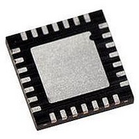
PIC18F27J13-I/ML Microchip Technology, PIC18F27J13-I/ML Datasheet - Page 38

PIC18F27J13-I/ML
Manufacturer Part Number
PIC18F27J13-I/ML
Description
IC PIC MCU 128KB FLASH 28QFN
Manufacturer
Microchip Technology
Series
PIC® XLP™ 18Fr
Datasheets
1.PIC18LF24J10-ISS.pdf
(32 pages)
2.PIC18F26J13-ISS.pdf
(496 pages)
3.PIC18F26J13-ISS.pdf
(558 pages)
4.PIC18F26J13-ISS.pdf
(12 pages)
Specifications of PIC18F27J13-I/ML
Core Size
8-Bit
Program Memory Size
128KB (64K x 16)
Core Processor
PIC
Speed
48MHz
Connectivity
I²C, LIN, SPI, UART/USART
Peripherals
Brown-out Detect/Reset, POR, PWM, WDT
Number Of I /o
22
Program Memory Type
FLASH
Ram Size
3.8K x 8
Voltage - Supply (vcc/vdd)
2.15 V ~ 3.6 V
Data Converters
A/D 10x10b/12b
Oscillator Type
Internal
Operating Temperature
-40°C ~ 85°C
Package / Case
*
Controller Family/series
PIC18
Cpu Speed
48MHz
Digital Ic Case Style
QFN
Supply Voltage Range
1.8V To 5.5V
Embedded Interface Type
I2C, SPI, USART
Rohs Compliant
Yes
Processor Series
PIC18F
Core
PIC
Data Bus Width
8 bit
Data Ram Size
4 KB
Interface Type
I2C, SPI, EUSART
Maximum Clock Frequency
48 MHz
Number Of Programmable I/os
19
Number Of Timers
8
Operating Supply Voltage
2 V to 3.6 V
Maximum Operating Temperature
+ 85 C
Mounting Style
SMD/SMT
3rd Party Development Tools
52715-96, 52716-328, 52717-734, 52712-325, EWPIC18
Development Tools By Supplier
DM164128, DM180021, DM183026-2, DV164131, MA180030, DM183022, DM183032, DV164136, MA180024
Minimum Operating Temperature
- 40 C
On-chip Adc
12 bit, 10 Channel
Lead Free Status / RoHS Status
Lead free / RoHS Compliant
For Use With
MA180030 - BOARD DEMO PIC18F47J13 FS USBMA180029 - BOARD DEMO PIC18F47J53 FS USB
Eeprom Size
-
Lead Free Status / Rohs Status
Details
Available stocks
Company
Part Number
Manufacturer
Quantity
Price
Company:
Part Number:
PIC18F27J13-I/ML
Manufacturer:
MICROCHIP
Quantity:
4 000
- PIC18LF24J10-ISS PDF datasheet
- PIC18F26J13-ISS PDF datasheet #2
- PIC18F26J13-ISS PDF datasheet #3
- PIC18F26J13-ISS PDF datasheet #4
- Current page: 38 of 558
- Download datasheet (5Mb)
external clock source to be connected to the OSC1 pin.
PIC18F47J13 FAMILY
3.2.3
The EC and ECPLL Oscillator modes require an
There is no oscillator start-up time required after a
Power-on Reset (POR) or after an exit from Sleep mode.
In the EC Oscillator mode, the oscillator frequency,
divided by 4, is available on the OSC2 pin. In the
ECPLL Oscillator mode, the PLL output, divided by 4,
is available on the OSC2 pin. This signal may be used
for test purposes or to synchronize other logic.
Figure 3-3 displays the pin connections for the EC
Oscillator mode.
FIGURE 3-3:
3.2.4
A Phase Locked Loop (PLL) circuit provides an option for
users who want to use a low-frequency oscillator circuit
or clock the device up to its highest rated frequency from
a crystal oscillator. This may be useful for customers who
are concerned with EMI due to high-frequency crystals or
users who require higher clock speeds from the internal
oscillator. PIC18F47J13 family devices include two PLL
circuits: a 4x PLL and a 96 MHz PLL.
Either PLL can be enabled in HSPLL, ECPLL,
INTOSCPLL and INTOSCPLLO Oscillator modes by
setting the PLLEN bit (OSCTUNE<6>) or by clearing
the CFGPLLEN bit (CONFIG1L<4>).
The 96 MHz PLL is designed to produce a fixed
96 MHz reference clock from a fixed 4 MHz input. The
output can then be divided and used for producing a
48 MHz microcontroller core clock. Because the PLL
has a fixed frequency input and output, there are eight
prescaling options to match the oscillator input fre-
quency to the PLL. This prescaler allows the PLL to be
used with crystals, resonators and external clocks,
which are integer multiple frequencies of 4 MHz. For
example, a 12 MHz crystal could be used in a prescaler
Divide-by-Three mode to drive the 96 MHz PLL.
DS39974A-page 38
Clock from
Ext. System
EXTERNAL CLOCK INPUT
PLL FREQUENCY MULTIPLIER
F
OSC
/4
EXTERNAL CLOCK INPUT
OPERATION (EC AND
ECPLL CONFIGURATION)
OSC1/CLKI
OSC2/CLKO
PIC18F47J13
Preliminary
The 4x PLL is designed to produce variable reference
clocks of 16 to 48 MHz from any input clock between
4 and 12 MHz. The PLLSEL (CONFIG3H<2>) Config-
uration bit is used to select which PLL circuit will be
used by the application.
3.2.5
The PIC18F47J13 family devices include an internal
oscillator block which generates two different clock
signals; either can be used as the microcontroller’s
clock source. The internal oscillator may eliminate the
need for external oscillator circuits on the OSC1 and/or
OSC2 pins.
The main output (INTOSC) is an 8 MHz clock source
which can be used to directly drive the device clock. It
also drives the INTOSC postscaler which can provide a
range of clock frequencies from 31 kHz to 8 MHz.
Additionally, the INTOSC may be used in conjunction
with a PLL to generate clock frequencies up to 48 MHz.
The other clock source is the internal RC oscillator
(INTRC) which provides a nominal 31 kHz output.
INTRC is enabled if it is selected as the device clock
source. It is also enabled automatically when any of the
following are enabled:
• Power-up Timer
• Fail-Safe Clock Monitor
• Watchdog Timer
• Two-Speed Start-up
These features are discussed in larger detail in
Section 27.0 “Special Features of the CPU”.
The clock source frequency (INTOSC direct, INTRC
direct or INTOSC postscaler) is selected by configuring
the IRCF bits of the OSCCON register (page 42).
INTERNAL OSCILLATOR BLOCK
2010 Microchip Technology Inc.
Related parts for PIC18F27J13-I/ML
Image
Part Number
Description
Manufacturer
Datasheet
Request
R

Part Number:
Description:
Manufacturer:
Microchip Technology Inc.
Datasheet:

Part Number:
Description:
Manufacturer:
Microchip Technology Inc.
Datasheet:

Part Number:
Description:
Manufacturer:
Microchip Technology Inc.
Datasheet:

Part Number:
Description:
Manufacturer:
Microchip Technology Inc.
Datasheet:

Part Number:
Description:
Manufacturer:
Microchip Technology Inc.
Datasheet:

Part Number:
Description:
Manufacturer:
Microchip Technology Inc.
Datasheet:

Part Number:
Description:
Manufacturer:
Microchip Technology Inc.
Datasheet:

Part Number:
Description:
Manufacturer:
Microchip Technology Inc.
Datasheet:


