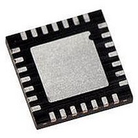
PIC18F27J13-I/ML Microchip Technology, PIC18F27J13-I/ML Datasheet - Page 143

PIC18F27J13-I/ML
Manufacturer Part Number
PIC18F27J13-I/ML
Description
IC PIC MCU 128KB FLASH 28QFN
Manufacturer
Microchip Technology
Series
PIC® XLP™ 18Fr
Datasheets
1.PIC18LF24J10-ISS.pdf
(32 pages)
2.PIC18F26J13-ISS.pdf
(496 pages)
3.PIC18F26J13-ISS.pdf
(558 pages)
4.PIC18F26J13-ISS.pdf
(12 pages)
Specifications of PIC18F27J13-I/ML
Core Size
8-Bit
Program Memory Size
128KB (64K x 16)
Core Processor
PIC
Speed
48MHz
Connectivity
I²C, LIN, SPI, UART/USART
Peripherals
Brown-out Detect/Reset, POR, PWM, WDT
Number Of I /o
22
Program Memory Type
FLASH
Ram Size
3.8K x 8
Voltage - Supply (vcc/vdd)
2.15 V ~ 3.6 V
Data Converters
A/D 10x10b/12b
Oscillator Type
Internal
Operating Temperature
-40°C ~ 85°C
Package / Case
*
Controller Family/series
PIC18
Cpu Speed
48MHz
Digital Ic Case Style
QFN
Supply Voltage Range
1.8V To 5.5V
Embedded Interface Type
I2C, SPI, USART
Rohs Compliant
Yes
Processor Series
PIC18F
Core
PIC
Data Bus Width
8 bit
Data Ram Size
4 KB
Interface Type
I2C, SPI, EUSART
Maximum Clock Frequency
48 MHz
Number Of Programmable I/os
19
Number Of Timers
8
Operating Supply Voltage
2 V to 3.6 V
Maximum Operating Temperature
+ 85 C
Mounting Style
SMD/SMT
3rd Party Development Tools
52715-96, 52716-328, 52717-734, 52712-325, EWPIC18
Development Tools By Supplier
DM164128, DM180021, DM183026-2, DV164131, MA180030, DM183022, DM183032, DV164136, MA180024
Minimum Operating Temperature
- 40 C
On-chip Adc
12 bit, 10 Channel
Lead Free Status / RoHS Status
Lead free / RoHS Compliant
For Use With
MA180030 - BOARD DEMO PIC18F47J13 FS USBMA180029 - BOARD DEMO PIC18F47J53 FS USB
Eeprom Size
-
Lead Free Status / Rohs Status
Details
Available stocks
Company
Part Number
Manufacturer
Quantity
Price
Company:
Part Number:
PIC18F27J13-I/ML
Manufacturer:
MICROCHIP
Quantity:
4 000
- PIC18LF24J10-ISS PDF datasheet
- PIC18F26J13-ISS PDF datasheet #2
- PIC18F26J13-ISS PDF datasheet #3
- PIC18F26J13-ISS PDF datasheet #4
- Current page: 143 of 558
- Download datasheet (5Mb)
REGISTER 10-4:
10.2
PORTA is a 7-bit wide, bidirectional port. It may
function as a 5-bit port, depending on the oscillator
mode selected. Setting a TRISA bit (= 1) will make the
corresponding PORTA pin an input (i.e., put the
corresponding output driver in a High-Impedance
mode). Clearing a TRISA bit (= 0) will make the
corresponding PORTA pin an output (i.e., put the
contents of the output latch on the selected pin).
Reading the PORTA register reads the status of the
pins, whereas writing to it, will write to the port latch.
The Data Latch (LATA) register is also memory mapped.
Read-modify-write operations on the LATA register read
and write the latched output value for PORTA.
The other PORTA pins are multiplexed with analog
inputs, the analog V
parator voltage reference output. The operation of pins,
RA<3:0> and RA5, as A/D Converter inputs is selected
by clearing or setting the control bits in the ANCON0
register (A/D Port Configuration Register 0).
The RAx pins may also be used as comparator inputs
by setting the appropriate bits in the CMxCON registers.
To use RAx as digital inputs, it is necessary to turn off
the comparators.
2010 Microchip Technology Inc.
bit 7
Legend:
R = Readable bit
-n = Value at POR
bit 7-3
bit 2-1
bit 0
Note 1:
Note:
U-0
—
PORTA, TRISA and LATA Registers
To enable the actual RTCC output, the RTCOE (RTCCFG<2>) bit needs to be set.
On a Power-on Reset (POR), RA5 and
RA<3:0> are configured as analog inputs
and read as ‘0’.
Unimplemented: Read as ‘0’
RTSECSEL<1:0>: RTCC Seconds Clock Output Select bits
11 = Reserved; do not use
10 = RTCC source clock is selected for the RTCC pin (can be INTRC, T1OSC or T1CKI depending
01 = RTCC seconds clock is selected for the RTCC pin
00 = RTCC alarm pulse is selected for the RTCC pin
PMPTTL: PMP Module TTL Input Buffer Select bit
1 = PMP module uses TTL input buffers
0 = PMP module uses Schmitt Trigger input buffers
U-0
REF
—
upon the RTCOSC (CONFIG3L<1>) and T1OSCEN (T1CON<3>) bit settings)
PADCFG1: PAD CONFIGURATION CONTROL REGISTER 1 (BANKED F3Ch)
+ and V
W = Writable bit
‘1’ = Bit is set
REF
U-0
—
- inputs and the com-
U-0
—
Preliminary
U = Unimplemented bit, read as ‘0’
‘0’ = Bit is cleared
U-0
—
PIC18F47J13 FAMILY
All PORTA pins have TTL input levels and full CMOS
output drivers.
The TRISA register controls the direction of the PORTA
pins, even when they are being used as analog inputs.
The user must ensure the bits in the TRISA register are
maintained set when using them as analog inputs.
EXAMPLE 10-2:
CLRF
CLRF
MOVLB
MOVLW
MOVWF
MOVLW
MOVWF
RTSECSEL1
PORTA
LATA
0x0F
0x0F
ANCON0 ; for digital inputs
0xCF
TRISA
R/W-0
(1)
; Initialize PORTA by
; clearing output
; data latches
; Alternate method
; to clear output
; data latches
; ANCONx register not in
; Access Bank
; Configure A/D
; Value used to
; initialize data
; direction
; Set RA<3:0> as inputs
; RA<5:4> as outputs
(1)
INITIALIZING PORTA
RTSECSEL0
x = Bit is unknown
R/W-0
DS39974A-page 143
(1)
PMPTTL
R/W-0
bit 0
Related parts for PIC18F27J13-I/ML
Image
Part Number
Description
Manufacturer
Datasheet
Request
R

Part Number:
Description:
Manufacturer:
Microchip Technology Inc.
Datasheet:

Part Number:
Description:
Manufacturer:
Microchip Technology Inc.
Datasheet:

Part Number:
Description:
Manufacturer:
Microchip Technology Inc.
Datasheet:

Part Number:
Description:
Manufacturer:
Microchip Technology Inc.
Datasheet:

Part Number:
Description:
Manufacturer:
Microchip Technology Inc.
Datasheet:

Part Number:
Description:
Manufacturer:
Microchip Technology Inc.
Datasheet:

Part Number:
Description:
Manufacturer:
Microchip Technology Inc.
Datasheet:

Part Number:
Description:
Manufacturer:
Microchip Technology Inc.
Datasheet:


