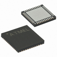
ATMEGA8535L-8MU Atmel, ATMEGA8535L-8MU Datasheet - Page 149

ATMEGA8535L-8MU
Manufacturer Part Number
ATMEGA8535L-8MU
Description
IC AVR MCU 8K 8MHZ 3V 44-QFN
Manufacturer
Atmel
Series
AVR® ATmegar
Specifications of ATMEGA8535L-8MU
Core Processor
AVR
Core Size
8-Bit
Speed
8MHz
Connectivity
I²C, SPI, UART/USART
Peripherals
Brown-out Detect/Reset, POR, PWM, WDT
Number Of I /o
32
Program Memory Size
8KB (4K x 16)
Program Memory Type
FLASH
Eeprom Size
512 x 8
Ram Size
512 x 8
Voltage - Supply (vcc/vdd)
2.7 V ~ 5.5 V
Data Converters
A/D 8x10b
Oscillator Type
Internal
Operating Temperature
-40°C ~ 85°C
Package / Case
44-VQFN Exposed Pad
Processor Series
ATMEGA8x
Core
AVR8
Data Bus Width
8 bit
Data Ram Size
512 B
Interface Type
SPI, TWI, UART
Maximum Clock Frequency
8 MHz
Number Of Programmable I/os
32
Number Of Timers
3
Operating Supply Voltage
2.7 V to 5.5 V
Maximum Operating Temperature
+ 85 C
Mounting Style
SMD/SMT
3rd Party Development Tools
EWAVR, EWAVR-BL
Minimum Operating Temperature
- 40 C
On-chip Adc
10 bit, 8 Channel
Package
44MLF EP
Device Core
AVR
Family Name
ATmega
Maximum Speed
8 MHz
For Use With
ATSTK600-DIP40 - STK600 SOCKET/ADAPTER 40-PDIP770-1007 - ISP 4PORT ATMEL AVR MCU SPI/JTAGATAVRISP2 - PROGRAMMER AVR IN SYSTEMATSTK500 - PROGRAMMER AVR STARTER KIT
Lead Free Status / RoHS Status
Lead free / RoHS Compliant
Available stocks
Company
Part Number
Manufacturer
Quantity
Price
Part Number:
ATMEGA8535L-8MU
Manufacturer:
ATMEL/爱特梅尔
Quantity:
20 000
- Current page: 149 of 321
- Download datasheet (3Mb)
Synchronous Clock Operation When Synchronous mode is used (UMSEL = 1), the XCK pin will be used as either clock
Frame Formats
2502K–AVR–10/06
input (Slave) or clock output (Master). The dependency between the clock edges and
data sampling or data change is the same. The basic principle is that data input (on
RxD) is sampled at the opposite XCK clock edge of the edge the data output (TxD) is
changed.
Figure 71. Synchronous Mode XCK Timing
The UCPOL bit UCRSC selects which XCK clock edge is used for data sampling and
which is used for data change. As Figure 71 shows, when UCPOL is zero the data will
be changed at rising XCK edge and sampled at falling XCK edge. If UCPOL is set, the
data will be changed at falling XCK edge and sampled at rising XCK edge.
A serial frame is defined to be one character of data bits with synchronization bits (start
and stop bits), and optionally a parity bit for error checking. The USART accepts all 30
combinations of the following as valid frame formats:
•
•
•
•
A frame starts with the start bit followed by the least significant data bit. Then the next
data bits, up to a total of nine, are succeeding, ending with the most significant bit. If
enabled, the parity bit is inserted after the data bits, before the stop bits. When a com-
plete frame is transmitted, it can be directly followed by a new frame, or the
communication line can be set to an idle (high) state. Figure 72 illustrates the possible
combinations of the frame formats. Bits inside brackets are optional.
Figure 72. Frame Formats
St
(n)
P
UCPOL = 1
UCPOL = 0
1 start bit
5, 6, 7, 8, or 9 data bits
no even or odd parity bit
1 or 2 stop bits
(IDLE)
Start bit, always low.
Data bits (0 to 8).
Parity bit. Can be odd or even.
RxD / TxD
RxD / TxD
St
XCK
XCK
0
1
2
3
4
FRAME
[5]
[6]
[7]
[8]
ATmega8535(L)
[P]
Sample
Sample
Sp1 [Sp2]
(St / IDLE)
149
Related parts for ATMEGA8535L-8MU
Image
Part Number
Description
Manufacturer
Datasheet
Request
R

Part Number:
Description:
IC AVR MCU 2.4GHZ XCEIVER 64QFN
Manufacturer:
Atmel
Datasheet:

Part Number:
Description:
Manufacturer:
Atmel
Datasheet:

Part Number:
Description:
MCU ATMEGA644/AT86RF230 40-DIP
Manufacturer:
Atmel
Datasheet:

Part Number:
Description:
BUNDLE ATMEGA644P/AT86RF230 QFN
Manufacturer:
Atmel
Datasheet:

Part Number:
Description:
BUNDLE ATMEGA644P/AT86RF230 TQFP
Manufacturer:
Atmel
Datasheet:

Part Number:
Description:
MCU ATMEGA1281/AT86RF230 64-TQFP
Manufacturer:
Atmel
Datasheet:

Part Number:
Description:
MCU ATMEGA1280/AT86RF230 100TQFP
Manufacturer:
Atmel
Datasheet:

Part Number:
Description:
BUNDLE ATMEGA1280/AT86RF100-TQFP
Manufacturer:
Atmel
Datasheet:

Part Number:
Description:
BUNDLE ATMEGA2560V/AT86RF230-ZU
Manufacturer:
Atmel
Datasheet:

Part Number:
Description:
MCU ATMEGA2561/AT86RF230 64-TQFP
Manufacturer:
Atmel
Datasheet:

Part Number:
Description:
INTERVAL AND WIPE/WASH WIPER CONTROL IC WITH DELAY
Manufacturer:
ATMEL Corporation
Datasheet:

Part Number:
Description:
Low-Voltage Voice-Switched IC for Hands-Free Operation
Manufacturer:
ATMEL Corporation
Datasheet:

Part Number:
Description:
MONOLITHIC INTEGRATED FEATUREPHONE CIRCUIT
Manufacturer:
ATMEL Corporation
Datasheet:

Part Number:
Description:
AM-FM Receiver IC U4255BM-M
Manufacturer:
ATMEL Corporation
Datasheet:


