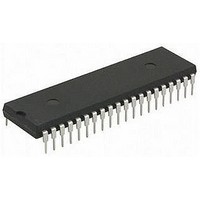
PIC16LF707-I/P Microchip Technology, PIC16LF707-I/P Datasheet - Page 63

PIC16LF707-I/P
Manufacturer Part Number
PIC16LF707-I/P
Description
MCU 8BIT 14KB FLASH 5.5V 40PDIP
Manufacturer
Microchip Technology
Series
PIC® XLP™ 16Fr
Specifications of PIC16LF707-I/P
Core Size
8-Bit
Program Memory Size
14KB (8K x 14)
Peripherals
Brown-out Detect/Reset, POR, PWM, WDT
Core Processor
PIC
Speed
20MHz
Connectivity
I²C, SPI, UART/USART
Number Of I /o
36
Program Memory Type
FLASH
Ram Size
363 x 8
Voltage - Supply (vcc/vdd)
1.8 V ~ 3.6 V
Data Converters
A/D 14x8b
Oscillator Type
Internal
Operating Temperature
-40°C ~ 85°C
Package / Case
40-DIP (0.600", 15.24mm)
Controller Family/series
PIC16LF
No. Of I/o's
36
Ram Memory Size
363Byte
Cpu Speed
20MHz
No. Of Timers
6
Processor Series
PIC16LF
Core
PIC
Data Bus Width
8 bit
Data Ram Size
368 B
Interface Type
I2C, SPI, AUSART
Maximum Clock Frequency
20 MHz
Number Of Programmable I/os
36
Number Of Timers
4
Operating Supply Voltage
1.8 V to 3.6 V
Maximum Operating Temperature
+ 85 C
Mounting Style
Through Hole
3rd Party Development Tools
52715-96, 52716-328, 52717-734
Development Tools By Supplier
PG164130, DV164035, DV244005, DV164005, PG164120, ICE2000
Minimum Operating Temperature
- 40 C
On-chip Adc
8 bit, 14 Channel
On-chip Dac
5 bit
Lead Free Status / RoHS Status
Lead free / RoHS Compliant
Eeprom Size
-
Lead Free Status / Rohs Status
Details
Available stocks
Company
Part Number
Manufacturer
Quantity
Price
Company:
Part Number:
PIC16LF707-I/PT
Manufacturer:
Microchip Technology
Quantity:
10 000
- Current page: 63 of 284
- Download datasheet (3Mb)
REGISTER 6-14:
REGISTER 6-15:
6.5.2
Each PORTD pin is multiplexed with other functions. The
pins and their combined functions are briefly described
here. For specific information about individual functions
such as the SSP, I
section in this data sheet.
6.5.2.1
These pins are configurable to function as one of the
following:
• General purpose I/O
• Capacitive sensing input
• Timer3 Gate input
6.5.2.2
These pins are configurable to function as one of the
following:
• General purpose I/O
• Capacitive sensing input
2010 Microchip Technology Inc.
bit 7
Legend:
R = Readable bit
-n = Value at POR
bit 7-0
bit 7
Legend:
R = Readable bit
-n = Value at POR
bit 7-0
Note 1:
TRISD7
ANSD7
R/W-1
R/W-1
When setting a pin to an analog input, the corresponding TRIS bit must be set to Input mode in order to
allow external control of the voltage on the pin.
PIN DESCRIPTIONS
RD0/CPSB5/T3G
RD1/CPSB6
ANSD<7:0>: Analog Select between Analog or Digital Function on Pins RD<7:0>, respectively
0 = Digital I/O. Pin is assigned to port or digital special function.
1 = Analog input. Pin is assigned as analog input
TRISD<7:0>: PORTD Tri-State Control bits
1 = PORTD pin configured as an input (tri-stated)
0 = PORTD pin configured as an output
2
C or interrupts, refer to the appropriate
ANSD6
TRISD6
R/W-1
R/W-1
TRISD: PORTD TRI-STATE REGISTER
ANSELD: PORTD ANALOG SELECT REGISTER
W = Writable bit
‘1’ = Bit is set
W = Writable bit
‘1’ = Bit is set
ANSD5
TRISD5
R/W-1
R/W-1
TRISD4
ANSD4
R/W-1
R/W-1
Preliminary
PIC16F707/PIC16LF707
U = Unimplemented bit, read as ‘0’
‘0’ = Bit is cleared
U = Unimplemented bit, read as ‘0’
‘0’ = Bit is cleared
TRISD3
ANSD3
R/W-1
R/W-1
6.5.2.3
These pins are configurable to function as one of the
following:
• General purpose I/O
• Capacitive sensing input
6.5.2.4
These pins are configurable to function as one of the
following:
• General purpose I/O
• Capacitive sensing input
6.5.2.5
These pins are configurable to function as one of the
following:
• General purpose I/O
• Capacitive sensing input
(1)
. Digital input buffer disabled.
TRISD2
RD2/CPSB7
RD3/CPSA8
RD4/CPSA12
ANSD2
R/W-1
R/W-1
x = Bit is unknown
x = Bit is unknown
TRISD1
ANSD1
R/W-1
R/W-1
DS41418A-page 63
TRISD0
ANSD0
R/W-1
R/W-1
bit 0
bit 0
Related parts for PIC16LF707-I/P
Image
Part Number
Description
Manufacturer
Datasheet
Request
R

Part Number:
Description:
Manufacturer:
Microchip Technology Inc.
Datasheet:

Part Number:
Description:
Manufacturer:
Microchip Technology Inc.
Datasheet:

Part Number:
Description:
Manufacturer:
Microchip Technology Inc.
Datasheet:

Part Number:
Description:
Manufacturer:
Microchip Technology Inc.
Datasheet:

Part Number:
Description:
Manufacturer:
Microchip Technology Inc.
Datasheet:

Part Number:
Description:
Manufacturer:
Microchip Technology Inc.
Datasheet:

Part Number:
Description:
Manufacturer:
Microchip Technology Inc.
Datasheet:

Part Number:
Description:
Manufacturer:
Microchip Technology Inc.
Datasheet:


