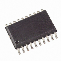
ATTINY26L-8SU Atmel, ATTINY26L-8SU Datasheet - Page 54

ATTINY26L-8SU
Manufacturer Part Number
ATTINY26L-8SU
Description
ID MCU AVR 2K 5V 8MHZ 20-SOIC
Manufacturer
Atmel
Series
AVR® ATtinyr
Specifications of ATTINY26L-8SU
Core Processor
AVR
Core Size
8-Bit
Speed
8MHz
Connectivity
USI
Peripherals
Brown-out Detect/Reset, POR, PWM, WDT
Number Of I /o
16
Program Memory Size
2KB (1K x 16)
Program Memory Type
FLASH
Eeprom Size
128 x 8
Ram Size
128 x 8
Voltage - Supply (vcc/vdd)
2.7 V ~ 5.5 V
Data Converters
A/D 11x10b
Oscillator Type
Internal
Operating Temperature
-40°C ~ 85°C
Package / Case
20-SOIC (7.5mm Width)
Package
20SOIC
Device Core
AVR
Family Name
ATtiny
Maximum Speed
8 MHz
Operating Supply Voltage
3.3|5 V
Data Bus Width
8 Bit
Number Of Programmable I/os
16
Interface Type
SPI/USI
On-chip Adc
11-chx10-bit
Number Of Timers
2
Cpu Family
ATtiny
Device Core Size
8b
Frequency (max)
8MHz
Total Internal Ram Size
128Byte
# I/os (max)
16
Number Of Timers - General Purpose
2
Operating Supply Voltage (typ)
3.3/5V
Operating Supply Voltage (max)
5.5V
Operating Supply Voltage (min)
2.7V
Instruction Set Architecture
RISC
Operating Temp Range
-40C to 85C
Operating Temperature Classification
Industrial
Mounting
Surface Mount
Pin Count
20
Package Type
SOIC
Processor Series
ATTINY2x
Core
AVR8
Data Ram Size
128 B
Maximum Clock Frequency
8 MHz
Maximum Operating Temperature
+ 85 C
Mounting Style
SMD/SMT
3rd Party Development Tools
EWAVR, EWAVR-BL
Development Tools By Supplier
ATAVRDRAGON, ATSTK500, ATSTK600, ATAVRISP2, ATAVRONEKIT
Minimum Operating Temperature
- 40 C
For Use With
ATSTK600-DIP40 - STK600 SOCKET/ADAPTER 40-PDIP770-1007 - ISP 4PORT ATMEL AVR MCU SPI/JTAG770-1004 - ISP 4PORT FOR ATMEL AVR MCU SPIATAVRISP2 - PROGRAMMER AVR IN SYSTEMATSTK505 - ADAPTER KIT FOR 14PIN AVR MCU
Lead Free Status / RoHS Status
Lead free / RoHS Compliant
Other names
ATTINY26L-8SJ
ATTINY26L-8SJ
ATTINY26L-8SJ
Available stocks
Company
Part Number
Manufacturer
Quantity
Price
Company:
Part Number:
ATTINY26L-8SU
Manufacturer:
Atmel
Quantity:
3 500
Part Number:
ATTINY26L-8SU
Manufacturer:
ATMEL/爱特梅尔
Quantity:
20 000
Table 27. Overriding Signals for Alternate Functions in PB7..PB4
Notes:
54
Signal
Name
PUOE
PUOV
DDOE
DDOV
PVOE
PVOV
DIEOE
DIEOV
DI
AIO
1. RSTDISBL Fuse (active low) is described in section “System Control and Reset” on page 32.
2. Note that the PCINT1 Interrupt is only enabled if both the Global Interrupt Flag is enabled, the PCIE1 flag in GIMSK is set
3. PB5IOENABLE and PB4IOENABLE are given by the PLLCK and CKSEL Fuses as described in “Clock Sources” on page
4. External low level interrupt is enabled if both the Global Interrupt Flag is enabled and the INT0 flag in GIMSK is set as
5. Not operator is marked with “~”.
6. The operation of the Timer/Counter0 with external clock disabled is described in “8-bit Timer/Counter0” on page 65.
7. External clock is selected by the PLLCK and CKSEL Fuses as described in “Clock Sources” on page 25.
ATtiny26(L)
and the alternate function of the pin is disabled as described in “Pin Change Interrupt” on page 62.
25.
described in “External Interrupt” on page 62.
PB7/ADC10/RESET/
PCINT1
RSTDSBL
1
RSTDSBL
0
0
0
PCINT1_ENABLE
PCINT1_ENABLE
~
PCINT1
ADC10, RESET INPUT
(5)
RSTDSBL
(1)
(1)
(1)
• DI/SDA/OC1A/PCINT0 – Port B, Bit 0
DI: Data Input in USI Three-wire mode. USI Three-wire mode does not override normal port
functions., so pin must be configure as an input.
SDA: Serial Data in USI Two-wire mode. Serial data pin is bi-directional and uses open-collector
output. The SDA pin is enabled by setting the pin as an output. The pin is pulled low when the
PORTB0 or USI shiftRegister is zero when DDB0 is set (one). Pull-up is disabled in USI Two-
wire mode.
OC1A: Inverted Timer/Counter1 PWM output A: The PB0 pin can serve as an Inverted output for
the PWM mode if not used in programming or USI. The PB0 pin has to be configured as an out-
put (DDB0 set (one)) to serve this function.
PCINT0: Pin Change Interrupt 0 pin. Pin change interrupt is enabled on pin when global interrupt
is enabled, pin change interrupt is enabled and the alternate functions do not mask the interrupt.
The masking alternate functions are the inverted output compare match output OC1A and USI
data DI or SDA. Digital input is enabled on pin PB0 also in SLEEP modes, if the pin change
interrupt is enabled and not masked by the alternate functions. Table 27 and Table 28 relate the
alternate functions of Port B to the overriding signals shown in “Alternate Port Functions” on
page 46.
(2)
(2)
| RSTDSBL
•
(1)
PB6/ADC9/INT0/TO/
PCINT1
0
0
0
0
0
0
~T0_EXT_CLOCK
PCINT1_ENABLE
INT0_ENABLE
1
INT0, T0, PCINT1
ADC9
(4)
(2)
(6)
|
•
PB5/ADC8/XTAL2/
PCINT1
~
0
~PB5IOENABLE
0
0
0
PCINT1_ENABLE
~PB5IOENABLE
PCINT1_ENABLE
PB5IOENABLE
PCINT1
ADC8, XTAL2
(5)
PB5IOENABLE
(3)
(3)
(3)
(2)
(2)
(3)
|
•
PB4/ADC7/XTAL1
~PB4IOENABLE
0
~PB4IOENABLE
0
0
0
PCINT_ ENABLE
~PB4IOENABLE
EXT_CLOCK_ENABLE
PCINT1_ENABLE
PB4IOENABLE
EXT_CLOCK_ENABLE
External Clock, PCINT1
XTAL1
1477K–AVR–08/10
(3)
(3)
(3)
(3)
|
(2)
(2)
|
•
|
(7)


