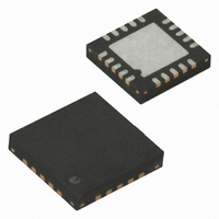
ATTINY44A-MU Atmel, ATTINY44A-MU Datasheet - Page 16

ATTINY44A-MU
Manufacturer Part Number
ATTINY44A-MU
Description
IC MCU AVR 4K FLASH 20MHZ 20QFN
Manufacturer
Atmel
Series
AVR® ATtinyr
Specifications of ATTINY44A-MU
Core Processor
AVR
Core Size
8-Bit
Speed
20MHz
Connectivity
USI
Peripherals
Brown-out Detect/Reset, POR, PWM, Temp Sensor, WDT
Number Of I /o
12
Program Memory Size
4KB (2K x 16)
Program Memory Type
FLASH
Eeprom Size
256 x 8
Ram Size
256 x 8
Voltage - Supply (vcc/vdd)
1.8 V ~ 5.5 V
Data Converters
A/D 8x10b
Oscillator Type
Internal
Operating Temperature
-40°C ~ 85°C
Package / Case
20-MLF®, QFN
Processor Series
ATTINY4x
Core
AVR8
Data Bus Width
8 bit
Data Ram Size
256 B
Interface Type
SPI/USI
Maximum Clock Frequency
20 MHz
Number Of Programmable I/os
12
Number Of Timers
2
Maximum Operating Temperature
+ 85 C
Mounting Style
SMD/SMT
3rd Party Development Tools
EWAVR, EWAVR-BL
Development Tools By Supplier
ATAVRDRAGON, ATSTK500, ATSTK600, ATAVRISP2, ATAVRONEKIT
Minimum Operating Temperature
- 40 C
On-chip Adc
20-ch x 10-bit
Data Rom Size
256 B
A/d Bit Size
10 bit
A/d Channels Available
20
Height
0.74 mm
Length
4 mm
Supply Voltage (max)
5.5 V
Supply Voltage (min)
1.8 V
Width
4 mm
For Use With
ATSTK600 - DEV KIT FOR AVR/AVR32770-1007 - ISP 4PORT ATMEL AVR MCU SPI/JTAGATAVRISP2 - PROGRAMMER AVR IN SYSTEM
Lead Free Status / RoHS Status
Lead free / RoHS Compliant
Available stocks
Company
Part Number
Manufacturer
Quantity
Price
Company:
Part Number:
ATTINY44A-MU
Manufacturer:
IXYS
Quantity:
2 291
Company:
Part Number:
ATTINY44A-MU
Manufacturer:
Atmel
Quantity:
30 143
Part Number:
ATTINY44A-MU
Manufacturer:
MICROCHIP/微芯
Quantity:
20 000
Part Number:
ATTINY44A-MUR
Manufacturer:
MICROCHIP/微芯
Quantity:
20 000
- Current page: 16 of 286
- Download datasheet (10Mb)
5.2.1
5.3
16
EEPROM Data Memory
ATtiny24A/44A/84A
Data Memory Access Times
When using register indirect addressing modes with automatic pre-decrement and post-incre-
ment, the address registers X, Y, and Z are decremented or incremented.
The 32 general purpose working registers, 64 I/O Registers, and the 128/256/512 bytes of inter-
nal data SRAM in the ATtiny24A/44A/84A are all accessible through all these addressing
modes. The Register File is described in
Figure 5-2.
This section describes the general access timing concepts for internal memory access. The
internal data SRAM access is performed in two clk
Figure 5-3.
The ATtiny24A/44A/84A contains 128/256/512 bytes of data EEPROM memory. It is organized
as a separate data space, in which single bytes can be read and written. The EEPROM has an
endurance of at least 100,000 write/erase cycles. The access between the EEPROM and the
CPU is described in the following, specifying the EEPROM Address Registers, the EEPROM
Data Register, and the EEPROM Control Register. For a detailed description of Serial data
downloading to the EEPROM, see
Address
clk
Data
Data
Data Memory Map
On-chip Data SRAM Access Cycles
WR
CPU
RD
(128/256/512 x 8)
64 I/O Registers
Compute Address
Data Memory
Internal SRAM
32 Registers
T1
Memory Access Instruction
“Serial Programming” on page
“General Purpose Register File” on page
0x0DF/0x015F/0x025F
0x0000 - 0x001F
0x0020 - 0x005F
0x0060
Address valid
CPU
T2
cycles as illustrated in
Next Instruction
162.
T3
Figure
8183C–AVR–03/11
9.
5-3.
Related parts for ATTINY44A-MU
Image
Part Number
Description
Manufacturer
Datasheet
Request
R

Part Number:
Description:
Manufacturer:
Atmel Corporation
Datasheet:

Part Number:
Description:
Manufacturer:
Atmel Corporation
Datasheet:

Part Number:
Description:
MCU AVR 4K FLASH 15MHZ 20-QFN
Manufacturer:
Atmel
Datasheet:

Part Number:
Description:
IC MCU AVR 4K FLASH 20MHZ 20-QFN
Manufacturer:
Atmel
Datasheet:

Part Number:
Description:
IC MCU AVR 4K FLASH 20MHZ 14SOIC
Manufacturer:
Atmel
Datasheet:

Part Number:
Description:
MCU AVR 4KB FLASH 20MHZ 14SOIC
Manufacturer:
Atmel
Datasheet:

Part Number:
Description:
MCU AVR 4KB FLASH 20MHZ 20QFN
Manufacturer:
Atmel
Datasheet:

Part Number:
Description:
IC MCU AVR 4K FLASH 15MHZ 14SOIC
Manufacturer:
Atmel
Datasheet:

Part Number:
Description:
IC MCU AVR 4K FLASH 20MHZ 14-DIP
Manufacturer:
Atmel
Datasheet:

Part Number:
Description:
Manufacturer:
Atmel Corporation
Datasheet:

Part Number:
Description:
Microcontrollers (MCU) 512B FL 32B SRAM TIMER ATTINY4 12MHz
Manufacturer:
Atmel

Part Number:
Description:
IC MCU AVR 512B FLASH SOT-23-6
Manufacturer:
Atmel
Datasheet:

Part Number:
Description:
IC MCU AVR 512B FLASH SOT-23-6
Manufacturer:
Atmel
Datasheet:


