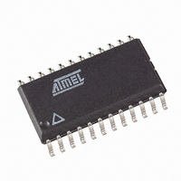
AT90PWM216-16SUR Atmel, AT90PWM216-16SUR Datasheet - Page 250

AT90PWM216-16SUR
Manufacturer Part Number
AT90PWM216-16SUR
Description
MCU AVR 16K FLASH 16MHZ 24SOIC
Manufacturer
Atmel
Series
AVR® 90PWM Lightingr
Datasheet
1.AT90PWM216-16SU.pdf
(359 pages)
Specifications of AT90PWM216-16SUR
Core Processor
AVR
Core Size
8-Bit
Speed
16MHz
Connectivity
SPI, UART/USART
Peripherals
Brown-out Detect/Reset, POR, PWM, WDT
Number Of I /o
19
Program Memory Size
16KB (16K x 8)
Program Memory Type
FLASH
Eeprom Size
512 x 8
Ram Size
1K x 8
Voltage - Supply (vcc/vdd)
2.7 V ~ 5.5 V
Data Converters
A/D 8x10b; D/A 1x10b
Oscillator Type
Internal
Operating Temperature
-40°C ~ 105°C
Package / Case
24-SOIC (7.5mm Width)
Processor Series
AT90PWMx
Core
AVR8
3rd Party Development Tools
EWAVR, EWAVR-BL
Development Tools By Supplier
ATAVRDRAGON, ATSTK500, ATSTK600, ATAVRISP2, ATAVRONEKIT, ATAVRFBKIT, ATAVRISP2
Lead Free Status / RoHS Status
Lead free / RoHS Compliant
- Current page: 250 of 359
- Download datasheet (6Mb)
21.8.2
250
AT90PWM216/316
ADC Control and Status Register A – ADCSRA
Table 21-4.
If these bits are changed during a conversion, the change will not take effect until this conversion
is complete (it means while the ADIF bit in ADCSRA register is set).
Bit
Read/Write
Initial Value
• Bit 7 – ADEN: ADC Enable Bit
Set this bit to enable the ADC.
Clear this bit to disable the ADC.
Clearing this bit while a conversion is running will take effect at the end of the conversion.
• Bit 6– ADSC: ADC Start Conversion Bit
Set this bit to start a conversion in single conversion mode or to start the first conversion in free
running mode.
Cleared by hardware when the conversion is complete. Writing this bit to zero has no effect.
The first conversion performs the initialization of the ADC.
• Bit 5 – ADATE: ADC Auto trigger Enable Bit
Set this bit to enable the auto triggering mode of the ADC.
Clear it to return in single conversion mode.
In auto trigger mode the trigger source is selected by the ADTS bits in the ADCSRB register.
See
• Bit 4– ADIF: ADC Interrupt Flag
Set by hardware as soon as a conversion is complete and the Data register are updated with the
conversion result.
Cleared by hardware when executing the corresponding interrupt handling vector.
Alternatively, ADIF can be cleared by writing it to logical one.
• Bit 3– ADIE: ADC Interrupt Enable Bit
Set this bit to activate the ADC end of conversion interrupt.
Clear it to disable the ADC end of conversion interrupt.
• Bit 2, 1, 0– ADPS2, ADPS1, ADPS0: ADC Prescaler Selection Bits
These 3 bits determine the division factor between the system clock frequency and input clock of
the ADC.
The different setting are shown in
MUX3
1
1
1
Table 21-6 on page
ADC Input Channel Selection
MUX2
1
1
1
ADEN
R/W
7
0
251.
ADSC
R/W
6
0
MUX1
0
1
1
ADATE
Table
R/W
5
0
21-5.
ADIF
R
MUX0
1
0
1
4
0
ADIE
R/W
3
0
Description
Reserved
Bandgap
GND
ADPS2
R/W
2
0
ADPS1
R/W
1
0
ADPS0
R/W
0
0
7710E–AVR–08/10
ADCSRA
Related parts for AT90PWM216-16SUR
Image
Part Number
Description
Manufacturer
Datasheet
Request
R

Part Number:
Description:
Manufacturer:
Atmel Corporation
Datasheet:

Part Number:
Description:
8-bit Microcontroller with 16K Bytes In-System Programmable flash
Manufacturer:
ATMEL [ATMEL Corporation]
Datasheet:

Part Number:
Description:
MCU AVR 16K ISP FLSH 16MHZ24SOIC
Manufacturer:
Atmel
Datasheet:

Part Number:
Description:
DEV KIT FOR AVR/AVR32
Manufacturer:
Atmel
Datasheet:

Part Number:
Description:
INTERVAL AND WIPE/WASH WIPER CONTROL IC WITH DELAY
Manufacturer:
ATMEL Corporation
Datasheet:

Part Number:
Description:
Low-Voltage Voice-Switched IC for Hands-Free Operation
Manufacturer:
ATMEL Corporation
Datasheet:

Part Number:
Description:
MONOLITHIC INTEGRATED FEATUREPHONE CIRCUIT
Manufacturer:
ATMEL Corporation
Datasheet:

Part Number:
Description:
AM-FM Receiver IC U4255BM-M
Manufacturer:
ATMEL Corporation
Datasheet:

Part Number:
Description:
Monolithic Integrated Feature Phone Circuit
Manufacturer:
ATMEL Corporation
Datasheet:

Part Number:
Description:
Multistandard Video-IF and Quasi Parallel Sound Processing
Manufacturer:
ATMEL Corporation
Datasheet:

Part Number:
Description:
High-performance EE PLD
Manufacturer:
ATMEL Corporation
Datasheet:

Part Number:
Description:
8-bit Flash Microcontroller
Manufacturer:
ATMEL Corporation
Datasheet:


