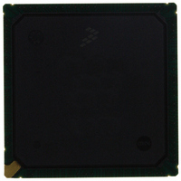
MCF5474VR200 Freescale Semiconductor, MCF5474VR200 Datasheet - Page 6

MCF5474VR200
Manufacturer Part Number
MCF5474VR200
Description
IC MPU 32BIT COLDF 388-PBGA
Manufacturer
Freescale Semiconductor
Series
MCF547xr
Datasheet
1.MCF5472VR200.pdf
(34 pages)
Specifications of MCF5474VR200
Core Processor
Coldfire V4E
Core Size
32-Bit
Speed
200MHz
Connectivity
EBI/EMI, Ethernet, I²C, SPI, UART/USART, USB
Peripherals
DMA, PWM, WDT
Number Of I /o
99
Program Memory Type
ROMless
Ram Size
32K x 8
Voltage - Supply (vcc/vdd)
1.43 V ~ 1.58 V
Oscillator Type
External
Operating Temperature
0°C ~ 70°C
Package / Case
388-BGA
Processor Series
MCF547x
Core
ColdFire V4
Data Bus Width
32 bit
Development Tools By Supplier
M5475EVBE
Maximum Clock Frequency
83 MHz
Operating Supply Voltage
3 V to 3.6 V
Maximum Operating Temperature
+ 70 C
3rd Party Development Tools
JLINK-CF-BDM26, EWCF
Data Ram Size
32 KB
Minimum Operating Temperature
0 C
Program Memory Size
64KB
Cpu Speed
200MHz
Embedded Interface Type
I2C, UART, DMA
Digital Ic Case Style
BGA
No. Of Pins
388
Rohs Compliant
Yes
For Use With
M5475EVBGHS - KIT DEV GHS FOR M5475EVBM5474GFE - MODULE M5474 FIRE ENGINEM5474LITEKIT - KIT DEV FOR MCF547X
Lead Free Status / RoHS Status
Lead free / RoHS Compliant
Eeprom Size
-
Program Memory Size
-
Data Converters
-
Lead Free Status / Rohs Status
Lead free / RoHS Compliant
Available stocks
Company
Part Number
Manufacturer
Quantity
Price
Company:
Part Number:
MCF5474VR200
Manufacturer:
Freescale Semiconductor
Quantity:
135
Company:
Part Number:
MCF5474VR200
Manufacturer:
Freescale Semiconductor
Quantity:
10 000
Hardware Design Considerations
4
4.1
To further enhance noise isolation, an external filter is strongly recommended for PLL analog V
Figure 2
close to the dedicated PLL V
4.2
Figure 3
(IV
6
1
2
3
Output high voltage I
Output low voltage I
Capacitance
Input leakage current
DD
IV
example circuit. There are three PLL V
This specification is guaranteed by design and is not 100% tested.
Capacitance C
).
DD
should be connected between the board V
shows situations in sequencing the I/O V
and PLL V
Hardware Design Considerations
PLL Power Filtering
Supply Voltage Sequencing and Separation Cautions
3
, V
in
IN
DD
= 0 V, f = 1 MHz
is periodically sampled rather than 100% tested.
OL
OH
should be at the same voltage. PLL V
Characteristic
= 8 mA, 16 mA,24 mA
= 8 mA, 16 mA,24 mA
Board V
DD
pin as possible.
Table 4. DC Electrical Specifications (continued)
DD
MCF547x ColdFire
Figure 2. System PLL V
DD
10 Ω
inputs. A filter circuit should used on each PLL V
5
DD
DD
(EV
and the PLL V
10 µF
DD
GND
®
), SDRAM V
DD
Microprocessor, Rev. 4
should have a filtered input. Please see
Symbol
V
DD
V
C
I
DD
OH
OL
in
IN
Power Filter
pins. The resistor and capacitors should be placed as
DD
0.1 µF
(SD V
DD
–1.0
Min
), PLL V
2.4
PLL V
—
—
DD
DD
DD
Pin
DD
input.
(PLL V
pins. The filter shown in
Freescale Semiconductor
Max
TBD
0.5
1.0
Figure 2
—
DD
), and Core V
for an
Units
μA
pF
V
V
DD


