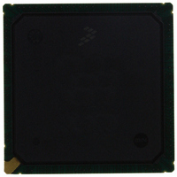
MCF5474VR200 Freescale Semiconductor, MCF5474VR200 Datasheet - Page 21

MCF5474VR200
Manufacturer Part Number
MCF5474VR200
Description
IC MPU 32BIT COLDF 388-PBGA
Manufacturer
Freescale Semiconductor
Series
MCF547xr
Datasheet
1.MCF5472VR200.pdf
(34 pages)
Specifications of MCF5474VR200
Core Processor
Coldfire V4E
Core Size
32-Bit
Speed
200MHz
Connectivity
EBI/EMI, Ethernet, I²C, SPI, UART/USART, USB
Peripherals
DMA, PWM, WDT
Number Of I /o
99
Program Memory Type
ROMless
Ram Size
32K x 8
Voltage - Supply (vcc/vdd)
1.43 V ~ 1.58 V
Oscillator Type
External
Operating Temperature
0°C ~ 70°C
Package / Case
388-BGA
Processor Series
MCF547x
Core
ColdFire V4
Data Bus Width
32 bit
Development Tools By Supplier
M5475EVBE
Maximum Clock Frequency
83 MHz
Operating Supply Voltage
3 V to 3.6 V
Maximum Operating Temperature
+ 70 C
3rd Party Development Tools
JLINK-CF-BDM26, EWCF
Data Ram Size
32 KB
Minimum Operating Temperature
0 C
Program Memory Size
64KB
Cpu Speed
200MHz
Embedded Interface Type
I2C, UART, DMA
Digital Ic Case Style
BGA
No. Of Pins
388
Rohs Compliant
Yes
For Use With
M5475EVBGHS - KIT DEV GHS FOR M5475EVBM5474GFE - MODULE M5474 FIRE ENGINEM5474LITEKIT - KIT DEV FOR MCF547X
Lead Free Status / RoHS Status
Lead free / RoHS Compliant
Eeprom Size
-
Program Memory Size
-
Data Converters
-
Lead Free Status / Rohs Status
Lead free / RoHS Compliant
Available stocks
Company
Part Number
Manufacturer
Quantity
Price
Company:
Part Number:
MCF5474VR200
Manufacturer:
Freescale Semiconductor
Quantity:
135
Company:
Part Number:
MCF5474VR200
Manufacturer:
Freescale Semiconductor
Quantity:
10 000
10
The PCI bus on the MCF54
refer to the PCI 2.2 spec for a more detailed timing analysis.
Freescale Semiconductor
Num
SDCSn,SDWE,
P1
P2
P3
P4
P5
P6
PCI Bus
SDBA[1:0]
RAS, CAS
SDADDR,
SDCLK0
SDCLK1
SDCLK0
SDCLK1
Frequency of Operation
Clock Period (t
Address, Data, and Command (33< PCI ≤ 66 Mhz)—Input Setup (t
Address, Data, and Command (0 < PCI ≤ 33 Mhz)—Input Setup (t
Address, Data, and Command (33–66 Mhz)—Output Valid (t
Address, Data, and Command (0–33 Mhz) - Output Valid (t
PCI signals (0–66 Mhz) - Output Hold (t
SDDATA
SDDATA
SDDQS
SDDQS
7
x is PCI 2.2 compliant. The following timing numbers are mostly from the PCI 2.2 spec. Please
CK
DD4
)
ROW
CMD
MCF547x ColdFire
Table 14. PCI Timing Specifications
Characteristic
DD1
Figure 17. DDR Read Timing
DD5
DH
)
®
COL
Microprocessor, Rev. 4
CL=2
CL=2.5
DV
DD2
DQS Read
DD10
DV
Preamble
)
)
DQS Read
DD3
Preamble
IS
IS
)
)
WD1 WD2 WD3 WD4
15.15
Min
3.0
7.0
25
—
—
0
WD1 WD2 WD3 WD4
DD9
Max
11.0
6.0
66
40
—
—
—
DQS Read
Postamble
MHz
Unit
ns
ns
ns
ns
ns
ns
DQS Read
Postamble
Notes
1
2
3
4
PCI Bus
21


