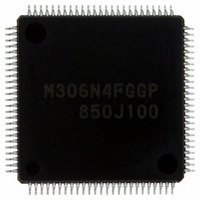
M306N4FGGP#U3 Renesas Electronics America, M306N4FGGP#U3 Datasheet - Page 80

M306N4FGGP#U3
Manufacturer Part Number
M306N4FGGP#U3
Description
IC M16C/6N4 MCU FLASH 100-LQFP
Manufacturer
Renesas Electronics America
Series
M16C™ M16C/6Nr
Specifications of M306N4FGGP#U3
Core Processor
M16C/60
Core Size
16-Bit
Speed
24MHz
Connectivity
CAN, I²C, IEBus, SIO, UART/USART
Peripherals
DMA, WDT
Number Of I /o
85
Program Memory Size
256KB (256K x 8)
Program Memory Type
FLASH
Ram Size
10K x 8
Voltage - Supply (vcc/vdd)
3 V ~ 5.5 V
Data Converters
A/D 26x10b; D/A 2x8b
Oscillator Type
Internal
Operating Temperature
-40°C ~ 85°C
Package / Case
100-LQFP
Package
100LQFP
Family Name
M16C
Maximum Speed
24 MHz
Operating Supply Voltage
3.3|5 V
Data Bus Width
16|32 Bit
Number Of Programmable I/os
87
Interface Type
I2C/UART
On-chip Adc
26-chx10-bit
On-chip Dac
2-chx8-bit
Number Of Timers
11
For Use With
R0K3306NKS001BE - KIT DEV RSK RSK-M16C/6NKR0K3306NKS000BE - KIT DEV RSK RSK-M16C/6NK
Lead Free Status / RoHS Status
Lead free / RoHS Compliant
Eeprom Size
-
Available stocks
Company
Part Number
Manufacturer
Quantity
Price
M16C/6N Group (M16C/6N4)
Rev.2.40
REJ03B0003-0240
Under development
This document is under development and its contents are subject to change.
NOTES:
Switching Characteristics
(Referenced to VCC = 3.3 V, VSS = 0 V, at Topr = –40 to 85 °C unless otherwise specified)
Table 5.67 Memory Expansion Mode and Microprocessor Mode (for 1- to 3-wait setting and external area access)
t
t
t
t
t
t
t
t
t
t
t
t
t
t
t
t
t
d(BCLK-AD)
h(BCLK-AD)
h(RD-AD)
h(WR-AD)
d(BCLK-CS)
h(BCLK-CS)
d(BCLK-ALE)
h(BCLK-ALE)
d(BCLK-RD)
h(BCLK-RD)
d(BCLK-WR)
h(BCLK-WR)
d(BCLK-DB)
h(BCLK-DB)
d(DB-WR)
h(WR-DB)
d(BCLK-HLDA)
Symbol
3. This standard value shows the timing when the
1. Calculated according to the BCLK frequency as follows:
2. Calculated according to the BCLK frequency as follows:
output is off, and does not show hold time of
data bus.
Hold time of data bus varies with capacitor volume
and pull-up (pull-down) resistance value.
Hold time of data bus is expressed in
t = – CR ✕ ln (1 – V
by a circuit of the right figure.
For example, when V
R =1 kΩ, hold time of output “L” level is
t = – 30 pF ✕ 1 kΩ ✕ ln (1 – 0.2 V
Aug 25, 2006
0.5 ✕ 10
f(BCLK)
(n – 0.5) ✕ 10
Address output delay time
Address output hold time (in relation to BCLK)
Address output hold time (in relation to RD)
Address output hold time (in relation to WR)
Chip select output delay time
Chip select output hold time (in relation to BCLK)
ALE signal output delay time
ALE signal output hold time
RD signal output delay time
RD signal output hold time
WR signal output delay time
WR signal output hold time
Data output delay time (in relation to BCLK)
Data output hold time (in relation to BCLK)
Data output delay time (in relation to WR)
Data output hold time (in relation to WR)
__________
HLDA output delay time
f(BCLK)
9
– 10 [ns]
page 78 of 88
9
– 40 [ns]
OL
OL
/ V
= 0.2 V
CC
Parameter
)
CC
/ V
CC
n is “1” for 1-wait setting, “2” for 2-wait setting and “3” for 3-wait setting.
When n = 1, f(BCLK) is 12.5 MHz or less.
CC
, C = 30 pF,
) = 6.7 ns.
(3)
(3)
Figure 5.21
Measuring
Condition
5. Electric Characteristics (Normal-ver.)
DBi
(NOTE 1)
(NOTE 2)
(NOTE 1)
Min.
–4
4
0
4
0
0
4
Standard
C
R
VCC = 3.3 V
Max.
30
30
25
30
30
40
40
Unit
ns
ns
ns
ns
ns
ns
ns
ns
ns
ns
ns
ns
ns
ns
ns
ns
ns


