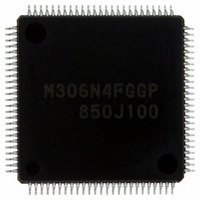
M306N4FGGP#U3 Renesas Electronics America, M306N4FGGP#U3 Datasheet - Page 14

M306N4FGGP#U3
Manufacturer Part Number
M306N4FGGP#U3
Description
IC M16C/6N4 MCU FLASH 100-LQFP
Manufacturer
Renesas Electronics America
Series
M16C™ M16C/6Nr
Specifications of M306N4FGGP#U3
Core Processor
M16C/60
Core Size
16-Bit
Speed
24MHz
Connectivity
CAN, I²C, IEBus, SIO, UART/USART
Peripherals
DMA, WDT
Number Of I /o
85
Program Memory Size
256KB (256K x 8)
Program Memory Type
FLASH
Ram Size
10K x 8
Voltage - Supply (vcc/vdd)
3 V ~ 5.5 V
Data Converters
A/D 26x10b; D/A 2x8b
Oscillator Type
Internal
Operating Temperature
-40°C ~ 85°C
Package / Case
100-LQFP
Package
100LQFP
Family Name
M16C
Maximum Speed
24 MHz
Operating Supply Voltage
3.3|5 V
Data Bus Width
16|32 Bit
Number Of Programmable I/os
87
Interface Type
I2C/UART
On-chip Adc
26-chx10-bit
On-chip Dac
2-chx8-bit
Number Of Timers
11
For Use With
R0K3306NKS001BE - KIT DEV RSK RSK-M16C/6NKR0K3306NKS000BE - KIT DEV RSK RSK-M16C/6NK
Lead Free Status / RoHS Status
Lead free / RoHS Compliant
Eeprom Size
-
Available stocks
Company
Part Number
Manufacturer
Quantity
Price
M16C/6N Group (M16C/6N4)
Rev.2.40
REJ03B0003-0240
Under development
This document is under development and its contents are subject to change.
2. Central Processing Unit (CPU)
Figure 2.1 CPU Registers
2.1 Data Registers (R0, R1, R2, and R3)
2.2 Address Registers (A0 and A1)
Figure 2.1 shows the CPU Registers. The CPU has 13 registers. Of these, R0, R1, R2, R3, A0, A1, and FB
configure a register bank. There are two register banks.
The R0 register consists of 16 bits, and is used mainly for transfers and arithmetic/logic operations. R1 to
R3 are the same as R0.
The R0 register can be separated between high (R0H) and low (R0L) for use as two 8-bit data registers.
R1H and R1L are the same as R0H and R0L. Conversely R2 and R0 can be combined for use as a 32-bit
data register (R2R0). R3R1 is analogous to R2R0.
The A0 register consists of 16 bits, and is used for address register indirect addressing and address
register relative addressing. They also are used for transfers and arithmetic/logic operations. A1 is the
same as A0.
In some instructions, A1 and A0 can be combined for use as a 32-bit address register (A1A0).
Aug 25, 2006
b31
NOTE:
1. These registers comprise a register bank. There are two register banks.
page 12 of 88
b15
R2
R3
IPL
b19
b19
The upper 4 bits of INTB are INTBH and the lower 16 bits of INTB are INTBL.
INTBH
b15
b15
b15
b15
R0H (R0's high bits) R0L (R0's low bits)
R1H (R1's high bits) R1L (R1's low bits)
b8
b7
U
I
PC
INTBL
O B S Z D C
USP
FLG
b8 b7
ISP
SB
R2
R3
A0
A1
FB
b0
b0
b0
b0
b0
b0
Interrupt Table Register
Program Counter
User Stack Pointer
Interrupt Stack Pointer
Static Base Register
Data Registers
Address Registers
Frame Base Registers
Flag Register
Carry Flag
Debug Flag
Zero Flag
Sign Flag
Register Bank Select Flag
Overflow Flag
Interrupt Enable Flag
Stack Pointer Select Flag
Reserved Area
Processor Interrupt Priority Level
Reserved Area
2. Central Processing Unit (CPU)
(1)
(1)
(1)


